I'm trying to make this circuit from here but I'm confused as the positive terminal of polarized capacitors is grounded. Can this be correct?
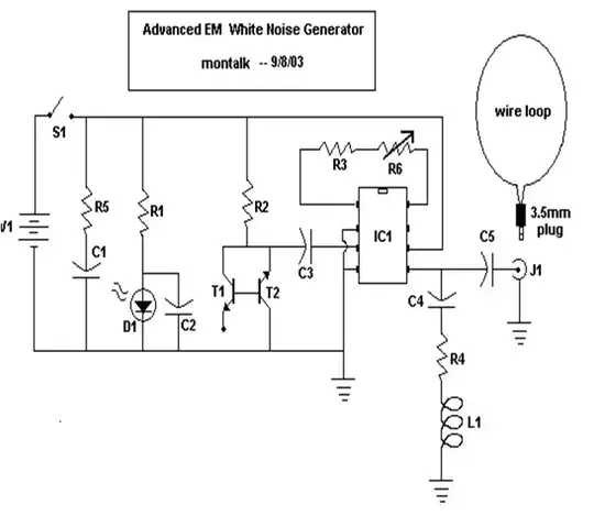
I'm trying to make this circuit from here but I'm confused as the positive terminal of polarized capacitors is grounded. Can this be correct?
For polarised capacitors they have adopted the convention that the curved plate is +ve.
T1-T2 are a noise source as this is a noise generator.
It is not unknown to use a reverse biased transistor junction as a white noise source. This tends to be voltage dependant and may need a minimum voltage to work. (From memory from 9 to 12V in some cases). He may have found that the 2N2222 works well enough at 9V.
It is possible that he has drawn his noise source "upside down" in error. If you invert the transistor array and adjust connections you get the circuit below which appears in a very large quantity of places as a noise source using reverse avalanche breakdown of the NP reverse biased junction to generate noise. If this is what is intended all mystery vanishes and this is a very standard circuit overall. In this case the noise source is in the feedback and bias path of the following transistor.

It's possible that the noise generator does in fact work "as shown" - it would be extremely easy to find out. His description of the noise generation process is "technically lacking" but odds are he found it by experiment of from other sources.
Other examples:
All of these use a single reverse biased pn junction rather than his interesting 2 transistor version. But the principle appears generally the same.
When I say "in feedback path" I mean that the noise junction is connected between an amplifier input (usually a transistor base ) and the amplifier output (eg collector) so the noise source is exposed to a varying voltage of its own inspiration./ "Not in fb path" means that the noise source sees DC and makes noise for amplification.
Pink noise generator - they say - noise source not in feedback path.
Used in a random number generator - noise source in feedback / bias path of next stagte.
Stacck exchange example questioning randomness
In RNG - in FB path. Note that this is mentioned in the post 2 down from here as going out of adjustment after a few months.
Another RNG in FB path
Another - not in FB path - and lo and behold it's the diagram from above with 18V with attribution removed.
For a change doing it digitally aka PRBS
Build your own synthesiser - noise source fed to op-amp