2

I just assembled a board that I have created that basically acts as a breakout board for a MKL26Z32VFM4. Today, I am trying to get it to communicate over SWD so I can program the initial bootloader. I've never done anything like this before and this is basically an experiment for myself to see what it takes to go from datasheet to working device with one of these microcontrollers.

I have another microcontroller emulating the SWD interface and it might not be emulating it properly (I haven't yet actually counted the pulses to make sure it is using 50 pulses to initialize). In any case, the KL26 failed to respond when I held RESET_b low.

I decided to see if the processor was even starting, so I put the oscilloscope on the RESET_b pin when it was left floating to see what would happen. According to the datasheet, it is pulled up internally and during the boot sequence it is driven low until the processor reaches a certain state. It then releases the pin and sees if it is rising fast enough (KL26 family reference, 6.3.3). If it isn't it keeps the processor in reset mode.

I see the following waveform on the RESET_b pin (pin PTA20):

RESET_b pin on channel 1

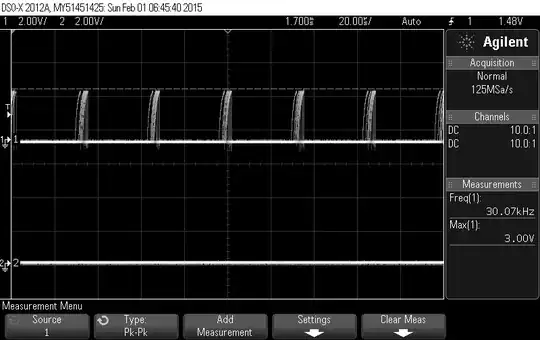
This doesn't look right at all. I should see it just simply high, not making a nice RC curve between 0 and 3V at approximately 30kHz (it's really wiggly as can be seen).

My theory: It is somehow stuck in a boot loop since it is driven low quite rapidly.

I could put a resistor on the reset to raise it to 3.3V, but I'm curious as to why this is happening. There are possibly a few mitigating factors:

  • This is my very first QFN chip that I have soldered by hand. I soldered it by tinning every pad, laying down flux, setting the chip on top, and then heating up a via-connected thermal pad on the back of the board for approximately 5 seconds while tapping the chip with tweezers. It appears to have soldered well and the 3.3V usb regulator seems to be working fine (at least the voltmeter and oscilloscope say so). It is possible that I have a void somewhere or a cold joint.
  • There was an ESD incident when the device was powered off and not connected to anything. I touched it with both hands to lift the board from my breadboard and felt a slight shock. The regulator still works and the chip doesn't let out smoke or heat up when powered on, so I'm not sure what happened here and if it is a problem. I have 2 additional backups that I could use, but that would require assembling them. I swear, if this is the problem I'm going to buy an ESD strap right away (yes I'm assembling this in my apartment, on a computer desk, sitting on a carpet, and it's cold outside (i.e. low humidity inside)).

In any case, my questions are:

  • How do I properly connect the chip for SWD? It's powered on, reset held low, and SWD connected to the appropriate pins, right? Am I missing something? My SWD program outputs 50 clock cycles, issues the SWD switchover command, outputs another 50 clock cycles, and attempts to read the IDCODE register.
  • What could be causing this strange RESET_b behavior? Did I break something and have to start over?

EDIT

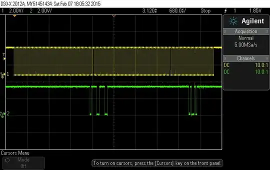
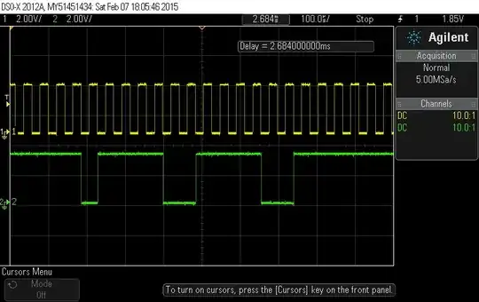
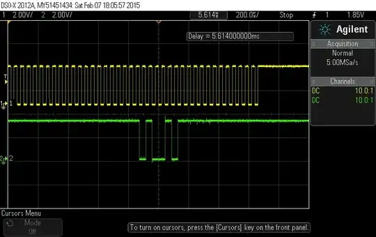
I have some additional waveforms from my programming attempt that might help. Clock frequency is 26Khz (KL26 says it can go up to 25Mhz).

Rise time on the SWD_CLK: 37nS (KL26 datasheet table 17 says this should be max 3ns...hmm) Rise time on clock

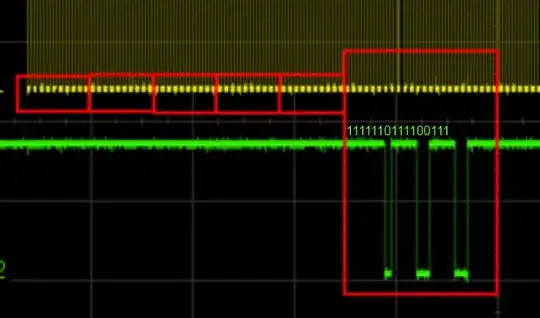
My transaction: 50 pulses, 16 bit switchover command, 50 pulses, read IDCODE Entire transaction

The switchover command: Switchover command

The read IDCODE command and lack of response from the KL26: Read IDCODE

Edit 2

Enabling the DSE bit on the PCR register for my SWD clock decreases the rise time to 7ns, still above 3ns. It also causes a ring that peaks at ~3.7V (the line settles at ~3.2V).

Los Frijoles
  • 2,202
  • 12
  • 21
  • I'm testing that tomorrow (sorry I take so long...I can only work on this during off-time). The ARM documentation seems to have a typo: both `0b0111100111100111` and `0b0011110011100111` are labeled as the JTAG-to-SWD sequence. One of them is actually the SWD-to-JTAG sequence. The section after says that if the JTAG-to-SWD command is executed twice in a debug session there could be unpredictable results requiring a POR. I'm going to be testing this as well since the device only supports SWD and might already be in that mode, making the switchover command a bad thing to use. – Los Frijoles Feb 13 '15 at 19:30
  • Switching to either mode is OK if both are reset and neither have been in use (POR), so I think the switchover is OK even though you don't have JTAG available. – Jon Feb 13 '15 at 20:21
  • Zooming into the second image, I'm counting 56 clocks before the leading 0. – Jon Feb 13 '15 at 20:22

1 Answers1

3

My SWD program outputs 50 clock cycles, issues the SWD switchover command,

Not accurate:
enter image description here

What could be causing this strange RESET_b behavior?

The reset behavior is normal for an un-programmed chip. It is crashing (main() returns) and being reset by the watchdog timer.


Here are a few general tips:

  1. First, check the errata for the part and family. There is nothing worse than wasting days chasing someone else's mistake. Facing a similar issue with a different Freescale chip, I discovered a number of issues it has with high slew rates during power up, especially on the reset pin. High slew rates may very well be causing a latch-up condition for you too.

  2. Use any available utility to attempt a mass-erase before further reprogramming.

  3. There is a tiny hint of "pins" visible along the vertical perimeter of the chips. Verify continuity between each "pin" and pad/trace/signal, using a needle and microscope, if necessary. Attach one continuity lead to the needle and, pushing toward the center of the chip and sliding downward, the needle will "catch" on the pin.

  4. When designing boards for hand-soldering QFN's, extend the pads well beyond the chip boundary. Give yourself enough room to use a regular fine-point soldering iron tip to fix errant pins. Initially, try doubling the pad length.

  5. With a small, but obvious, bubble of clean solder filling each pin, get rid of all flux and/or residue. Lightly scrub the chip and board with isopropyl alcohol until bright and shiny.

  6. It may be helpful to bake your circuit board (literally) and attempt re-flow on the pre-heated PCB.

  7. Lightly pressing down on the chip while hot will make the bubbles bulge out from under the chip slightly. Don't mash down so hard the bubbles overflow underneath the chip and short. Use a fine-point soldering iron to hit each bubble for a second and both the pad and chip will suck it up.

Remember that you don't have to mount your chip perfectly flat and... perfect.. like the machine does for it to work. It's OK if the chip is sitting up high and looks awkward; it's actually much easier to microscope in from the edge when it's elevated.

I wouldn't lose hope just yet, because the only way to brick them for good (with software) is to permanently secure them in a non-functional state. Although that could occur on a blank chip due to programming interruption/glitches, it is unlikely.

Jon
  • 742
  • 3
  • 12
  • KL26 reference manual, section 9.1 states: "Only one debug interface is supported: Serial Wire Debug (SWD)". I'm assuming the 50 cycles is to switch from JTAG to SWD, although the chip only supports and defaults to SWD on power up. – Jon Feb 05 '15 at 06:00
  • The 50 cycles alone are the line reset for SWD and are part of the initialization for the bus (I think it serves the purpose of clearing out all of the shift registers inside since no transaction is that long). The part that I think I may be able to cut out is the 16-bit switchover key from JTAG to SWD. I am pretty sure I was transmitting it (and everything else) backwards anyway. I won't have another chance to test until this weekend. – Los Frijoles Feb 05 '15 at 07:57
  • I suggest getting a FRDM-KL25Z or two. They are super cheap and you can install a SWD/JTAG header and use a cable to program many other chips/boards. Not to mention being able to switch SDA's in seconds! Edit: Now that I think about it, OpenSDA is open-sourced and does emulate SWD. Can you copy-and-paste it for now? – Jon Feb 06 '15 at 08:57
  • I'm probably going to buy one of those boards so I can have something to program these that I know works. I posted some additional waveforms from my programming attempt today. I think it is possible that my clock rise time is too long (causing the logic to glitch). I also couldn't find the OpenSDA source code, but I haven't yet searched deeply. – Los Frijoles Feb 08 '15 at 00:11
  • BTW, logical "on" is 0.7-0.75 Vdd. Trim your rise-time measurement to that voltage and see if the timing tends to agree more. If you have a bypass cap right next to the power pins, you should be ok. – Jon Feb 11 '15 at 02:43
  • +1 for the FRDM-KL25Z solution. This is what I ended up doing (and using the open-source USBDM firmware on the on-board OpenSDA debugger/programmer). It works, it works well, and it's cheap. MAKE SURE you update the OpenSDA *bootloader* or you may not be able to flash USBDM. That was a problem that cost me a few days. – akohlsmith Feb 13 '15 at 16:09