2

Spartan 6 clocking resources. The link here refers to the clocking resources of spartan-6 FPGA. I am using the DCM-CLKGEN primitive described in the link, to generate a 8x clock based on an input clock. It works fine as long as the input clock is stable.

But now i sweep the input clock at every 90 us by ±5%. I see that although the DCM does not lose lock, it takes very long (15 to 20 us) to change the output freq after changing the input frequency. This is for me undesirable. Any suggestions?

This question was posted on the xilinx forum and the suggestion was to reset the DCM everytime it loses lock. But the problem is that the DCM is not losing lock

Also, this was earlier posted on stackoverflow and now has been reposted here.
Sai Gautam
  • 109
  • 10
  • That's an interesting problem. I thought that input clock stability is the requirement. One of the Xilinx reps told me that the good clock should be 45ps p-p. – Nazar Jan 28 '15 at 15:15
  • @Naz Thanks...the input clock is stable, but is jumping frequency every 90 us. And I am sorry I did not understand the 45ps p-p requirement. Are you talking about rise or fall times? – Sai Gautam Jan 28 '15 at 15:37
  • I meant clock jitter, check [this](http://www.sitime.com/support2/documents/AN10007-Jitter-and-measurement.pdf) out. What do you mean by "jumping frequency every 90us"? – Nazar Jan 28 '15 at 15:54
  • @Naz lets say I start at 13.56 Mhz of input frequency, I then jump to 14.238Mhz after 90us, then to 12.88Mhz after 90 us, and so on. So in effect, I do a frequency modulation of my input frequency in a range of 13.56Mhz +/-5% – Sai Gautam Jan 28 '15 at 15:56
  • What is your intention to change the frequency in such a big range? For example SATA SSC (Spread Spectrum Clocking) uses only 5,000 ppm (0.5 %). A DCM lock can take up to 5 ms! – Paebbels Jan 28 '15 at 18:59
  • @Paebbels Originally the frequency to the input of the DCM was fixed and everything was working fine. The DCM is a small part of a big project to control the ignition and stability of a plasma chamber. The project has a microcontroller IC, a DSP IC and an FPGA IC and intercommunication is taking place. Now we sweep the frequency to the input of the DCM as described to enhance the stability of the chamber – Sai Gautam Jan 29 '15 at 07:53
  • Ok, but why do you chance the FPGA frequency? The FPGA is running at 2 MHz max. (14 MHz/8). What if you run the FPGA at 400 Mhz? That are 2.5 ns clock period so you can tune the output frequency in sub MHz steps. – Paebbels Jan 29 '15 at 08:23
  • @Paebbels the DCM input is NOT the FPGA clock. The FPGA has its own 100 Mhz clock... – Sai Gautam Jan 29 '15 at 08:44
  • So, what kind of settling time and/or accuracy do you actually need for the output clock relative to the input clock? Since the DCM is not meeting your needs, we need to know your actual requirements before we can suggest alternative approaches. – Dave Tweed Jan 29 '15 at 13:02
  • @DaveTweed The phase shift module inside the FPGA generates 16 signals from input clock and 8x clock, 4 gropus of 4 signals each at 0,90,180,270 degrees of shiftr plus some fine shifts all callibrated as register values – Sai Gautam Jan 29 '15 at 13:21
  • That doesn't answer my question. You've already addressed *what* you're trying to do. My question is about *how well* you need to do it. And I'm still confused about why you need to do this by reacting to an external clock, rather than simply generating all of these signals in parallel in the first place. – Dave Tweed Jan 29 '15 at 13:25
  • @DaveTweed The input clock comes from a DDS module controlled by a dsp IC outside the FPGA chip. This is fixed. Its the FPGAs job to generated 16 phase-shifted signals from this input clock signal – Sai Gautam Jan 29 '15 at 13:52
  • In that case, you'll have to use an external PLL/DLL to generate the 8x clock. But since you refuse to answer the question about the level of precision you need, I can't help you any further. – Dave Tweed Jan 29 '15 at 13:57
  • @DaveTweed The input clock is changing within 1 us, so ideally the multiplied clock must also change within this range of 1 us. Thiscannot be achieved by the onchip pll/dll – Sai Gautam Jan 29 '15 at 14:17
  • @DaveTweed can this be an alternative - make the external dds send the higher clock of 108.48 Mhz? – Sai Gautam Jan 29 '15 at 14:18
  • Yes, having the DDS generate the 8x clock would be a good approach, but since you said that the DSP+DDS part was "fixed", I assumed that this wasn't an option. You really need to be a lot more clear about the constraints under which you're working. Good luck! – Dave Tweed Jan 29 '15 at 14:45

3 Answers3

1

I am new to FPGAs, but I do not think this is the way to do it. From what I know, the main clock frequency should not change. If you want to use a part of FPGA as a asynchronous logic block, try to implement the clock divider by yourself toggling the slower clock on the rising edge process of the faster clock. Thus,

architecture
signal mainDiv2: sdt_logic;
signal mainDiv4: sdt_logic;
signal mainDiv8: sdt_logic;
begin
proc1: process(mainCLK)
begin
  if rising_edge(mainCLK) then mainDiv2 = not mainDiv2;
  end if;
end process proc1;

proc2: process(mainDiv2)
begin
  if rising_edge(mainDiv2) then mainDiv4 = not mainDiv4;
  end if;
end process proc2;

proc3: process(mainDiv4)
begin
  if rising_edge(mainDiv4) then mainDiv8 = not mainDiv8;
  end if;
end process proc3;

I have no idea if this will work. You should explore more on how to implement an FPGA for your particular application instead of trying to fix something that might be wrong to begin with. Let me know how it goes.

Nazar
  • 3,142
  • 4
  • 35
  • 62
  • However, if main clock get's locked-in automatically, you will have the same problem. Then, implementing a simple counter, as Dave Tweed suggested, is probably the way to go. – Nazar Jan 28 '15 at 21:25
  • The problem with counters is that I cannot multiply my clock. My DCM gives an Fout = Fin x 8 – Sai Gautam Jan 29 '15 at 08:22
1

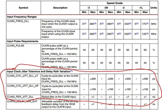
The DCM is optimized to provide a stable clock to the logic fabric. It isn't designed to deal with a modulated input frequency. On page 59 in the Spartan 6 DC and Switching Characteristics Datasheet you'll find these specs:

enter image description here

This question was posted on the xilinx forum and the suggestion was to reset the DCM everytime it loses lock. But the problem is that the DCM is not losing lock

Can you reset the DCM every time you change the input frequency? Be aware that after resetting the DCM it probably still takes many us to regain lock.

The Photon
  • 126,425
  • 3
  • 159
  • 304
  • You got that right. Thats what I tried testing and the problem is that the DCM cannot be reset under any circumstances as it creates a schort circuit at the transistors – Sai Gautam Jan 29 '15 at 08:20
1

The on-chip PLLs and DLLs of an FPGA are designed specifically to provide stable, low-jitter clocks to the internal logic, even if the external reference is not all that good. As such, the loop bandwidth is made as narrow as possible for maximum jitter attenuation, within the constraints of an on-chip implementation. They are NOT designed to be frequency-agile in the way that you are trying to use them.

If you just need to divide an input clock by 8, you shouldn't be using a DCM at all. All you need is a simple counter implemented in the fabric.

Dave Tweed
  • 168,369
  • 17
  • 228
  • 393
  • According to the doc linked by OP, the DCM in the Spartan 6 is DLL-based, not PLL. There are also PLL's, but it appears OP is using the DLL instead. – The Photon Jan 28 '15 at 21:44
  • @ThePhoton: It doesn't matter, the issues related to the control loop bandwidth and the suitability to the application at hand are still relevant. – Dave Tweed Jan 28 '15 at 21:56
  • @ThePhoton you are right the DCM is DLL based and not PLL based. The CMT of Spartan 6 provides 2 DCMs and 1 PLL. – Sai Gautam Jan 29 '15 at 08:15
  • @DaveTweed Thanks I get your point. You mean that the DLL/PLL on-chip is not designed to handle frequency jumps and produce the expected result. But I am trying to multiply my clock and not divide it. As in my Fout=Finx8. I cannot think of simple logics to do this – Sai Gautam Jan 29 '15 at 08:16
  • In that case, you need to edit your question so that it says "8x" instead of "divide-by-8". What do you use the 8x clock for? – Dave Tweed Jan 29 '15 at 12:13
  • @DaveTweed thank you...have edited the post. The input clock and the 8x clock are both fed to a phase shift module that phase shifts the input clock by the period of the 8x clock (45 degrees) – Sai Gautam Jan 29 '15 at 12:20
  • @DaveTweed input clock is at 13.56 Mhz and the 8x clock is at 108 Mhz. The FPFA sysclk is also at 108.48 Mhz. If I have to remove DCM I have to- (1)Increase my FPGA sysclk to a higher frequency and sample the input clock with sysclk. (2) I have to track the changes at the input clock (the +/-5% change). I do not know how to do this – Sai Gautam Jan 29 '15 at 12:23
  • It still isn't clear to me how all of this ties into your "plasma chamber" project. Wouldn't it be easier to generate the 45-degree shifted clock at the same time you generate the original swept clock? For example, there are DDS chips that can generate two signals simultaneously with arbitrary phase relationships between them. – Dave Tweed Jan 29 '15 at 12:58