12

I will freely admit that I am mainly digital when it comes to electronics, so may help explain my confusion (that or just general incompetence).

I am getting review feedback on a design, and one thing that keeps bugging me is that placing a BJT below the LED keeps being labelled as 'wrong'. Is this a major issue or just a convention or is the reviewer just being annoying?

schematic

simulate this circuit – Schematic created using CircuitLab

NOTE: The circuit is a sketch, ignore actual part numbers or values.

Oliver
  • 1,663
  • 1
  • 13
  • 23
  • 1
    The bjt placement is quite significant and can be the difference between a working and a not working circuit. Some informations about the piloting signal is required, the first scheme should be the safer though, it seems strange to me that it keeps reviewed. Perhaps you use PNP bjts? – Vladimir Cravero Jan 28 '15 at 11:42
  • Did you mean to use an NPN transistor in the right hand diagram? That would be unusual. – tomnexus Jan 28 '15 at 11:44
  • @Vladimir Cravero Yes, I meant an NPN BJT for both. – Oliver Jan 28 '15 at 11:47
  • The driving signal to the transistor base can be considered a standard logic input, with a voltage less than or equal to the LED VDD, and the resistor set so that current well over saturation is applied. In my mind, it's just going to work like a switch (ignoring transients), where you put the transistor shouldn't make a difference. – Oliver Jan 28 '15 at 11:49
  • 4
    Who labels the left one as wrong? The one on the right has the problem that you need a higher voltage at the base. If you have 3.3V logic, VDD=5V and a blue LED the left one will work, but not the right one. – starblue Jan 28 '15 at 12:18
  • 3
    Someone labelling a design as "wrong" without explanation or discussion in design review is being incredibly unhelpful. – pjc50 Jan 28 '15 at 12:24
  • 3
    Refer to these similar questions: [Why would one drive LEDs with a common emitter?](http://electronics.stackexchange.com/q/57845/33841) and [Good NPN configuration vs bad configuration](http://electronics.stackexchange.com/q/92891/33841) – alexan_e Jan 28 '15 at 13:50

3 Answers3

15

The significant difference here is where the currents go.

With a BJT, it doesn't just "act like a switch" - that is the end result you see at the high level, not what it actually does.

What actually happens is you apply a current to the base, and that then flows through the transistor and out of the emitter down to ground. At the same time it allows proportionally more current to flow from the collector down through the emitter to ground.

NPN and PNP transistor diagram with IB, IE and IC

We'll call these two currents \$I_B\$ and \$I_C\$ for the Base and Collector currents respectively.

enter image description here

So in the left hand schematic, the \$I_B\$ flows through the base resistor, then the BJT, and to ground. \$I_C\$ flows through the LED's resistor and the LED, then the BJT, and to ground. \$I_B\$ is set by the base resistor alone.

But, in the second circuit, \$I_B\$ flows through the base resistor, through the BJT, then through the LED's resistor and the LED. \$I_C\$ also flows through the BJT then through the LED's resistor and the LED. So the LED and its resistor get both \$I_B\$ and \$I_C\$.

Consequently the current \$I_B\$ is being set by both the base resistor and the LED's resistor, and also the voltage drop across the LED. Also the voltage drop across the LED's resistor is not just from \$I_C\$ but from both \$I_B\$ and \$I_C\$ combined.

Which is better? While the left-hand circuit is easier to understand, the right-hand circuit does have some advantages; in the schematic, the base current \$I_B\$ is set by two resistors and it may be possible to remove one of them (the base resistor) and just have the one resistor in the circuit to limit both the base current and the LED's current. That can save on parts, and if you have a lot of these circuits in you design that reduction in parts can soon add up.

Nick Bolton
  • 2,043
  • 8
  • 31
Majenko
  • 55,955
  • 9
  • 105
  • 187
  • 1
    Good answer. I was discussing this with a colleague and came to the same conclusion, the main difference is where the base current flows. I can see it being problematic though if the load is not a linear ohmic load, keeping a known good base current. However when cascading transistors or using simple loads I can see the benefit of a single resistor limiting both the load and the base current. – Oliver Jan 28 '15 at 12:30
  • 4
    Furthermore the right hand one (common collector) takes only as much *Ib* as is needed to drive the LED, while the left (common emitter) will consume as much *Ib* as R6 allows. Loading the input circuit less, arguably makes the "wrong" one better. –  Jan 28 '15 at 13:49
  • 2
    Adding to what Brian Drummond says above, since LEDs are current driven devices, the right hand circuit is often the appropriate choice (although I'd move the LED to the collector) because with a constant voltage applied to the base, the LED current can be set by the emitter resistor and will remain constant even if the power supply or the LED forward voltage varies. – lyndon Jan 28 '15 at 18:16
6

If your only goal is to get light out of the LED, then the circuit on the left is perfectly fine. The reason is because the voltage needed to change the state of the transistor is very low - typically around 0.7 V. However, the problem is that your LED is now at a "high" potential when the transistor is OPEN (called the "high-side" configuration). So what happens is that if you accidentally short the LED's cathode to ground, then it will immediately bypass the transistor and dump the full voltage across the device. This is perfectly avoidable if your LED is encased in some plastic box or something, but a very bad idea if the user can freely manipulate the thing (say, if your enclosure is a metal box). I've personally worked on applications where the LED is very expensive and this exact problem needs to be avoided.

The alternative is your circuit on the right. This is called the "low side" configuration. This avoids any potential damage to your device when it accidentally shorts out to other metal objects. However, the trade-off is that now the base voltage needs to get very high in order to change the state of the transistor from OPEN to SHORT. Remember that the voltage from the base to the emitter needs to be 0.7 V. But if the emitter is at, say, 5 V when current is flowing, then your base needs to get up to 5.5 V. This makes fast transitions very difficult.

Often times these problems are not very significant, and either configuration works. However, there are situations where neither is very effective. For example, if fast transitions are necessary, AND the LED needs to be protected against accidental shorts. Then you need to employ some more complicated variations, like using a high-side PNP instead of NPN. But we don't need to talk about that unless you want to hear it.

5

There are advantages and disadvantages to both techniques. There is also a special case where the right-hand circuit has a significant advantage.

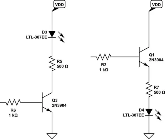
Left-hand circuit: A logic HI at the input results in a logic LO at the collector, which turns the LED on. The transistor acts as an inverter, which may be useful if the collector is driving another portion of the circuit (in addition to the LED).

Advantages:

1) turns ON with low control voltage. Basically, any voltage greater than Vbe (with suitable current limit resistor).

2) Transistor is saturated. This results in minimum heat generated by the transistor - this can be important if load current is high.

3) Power supply voltage that operates the LED can be a a different value than the logic voltage. This is often useful when operating the LED from a higher, un-regulated supply.


Right-hand circuit: a logic HI turns the LED on. However, this circuit is functioning as an emitter-follower. This has some consequences.

So long as the voltage at the collector of the transistor is equal to or higher than the chip logic HI voltage, the current through the LED is approximately equal to (V logic HI) - Vled - transistor Vbe drop - (tiny voltage drop across base resistor) all divided by the LED current limit resistor. Note that the base resistor is not needed in this application so long as you ensure that the voltage on the transistor collector is always equal to or greater than V logic supply.

Note the reduced voltage across the LED current limit resistor has to taken into account when calculating the value of that resistor.

Disadvantage: Power supply voltage at the collector has to be significantly higher than the sum of Vled & V logic HI. That specifically disallows this circuit from being used with low voltage logic.

There is a specific application where I prefer to use the emitter-follower configuration for driving LEDs. If you look closely at the emitter-follower configuration, you can think of it as a constant-current sink. Assuming that the output voltage from the chip always goes to V logic HI (CMOS output stage), you can set the LED current to whatever value is desired using just the emitter resistor. Note that this current doesn't change appreciably even if the transistor collector voltage is significantly higher than V logic.

This is useful when driving LEDs from an unregulated power supply. For example, a DC power supply derived from a 12Vac transformer with bridge rectifier and filter cap will have an output voltage between 12Vdc through about 20Vdc, assuming input line voltage variation of plus minus 20%.

I run my PIC projects with 5Vdc rail with unregulated supply voltages ranging from 12V through about 40Vdc. The PIC power supply is tiny - only capable of a few mA. I power all the LEDs and relays in the circuit from the unregulated supply. Using the emitter-follower LED driver keeps the PIC supply current to the minimum required and keeps the LED brightness constant even as the supply voltage varies.

ardnew
  • 115
  • 6
Dwayne Reid
  • 23,390
  • 2
  • 35
  • 67
  • +1 ... Nice point about the current-regulation of the second circuit. – Tut Jan 28 '15 at 21:48
  • 2
    Note [this answer](http://electronics.stackexchange.com/a/57849/25328) which offers a improvement on the second circuit by moving the LED to the collector side. – Tut Jan 28 '15 at 21:56
  • **Seems like the right place to ask**: To drive a LED strip with a 1k potentiometer, do I use common collector or emitter? The potentiometer goes on a voltage divider at the base, I suppose... But as the Ri or the Ro ? – Lucas BS Feb 07 '23 at 13:35
  • 1
    Try it both ways and see what happens. Both will work but having the LEDs in the Collector path results in a wider range of the pot travel being useful. Be sure the top of the pot is fed from a stable voltage source. Pick the Emitter resistor to set the maximum current through the LEDs. – Dwayne Reid Feb 07 '23 at 16:46
  • Thank you. Will do. There won't be a load resistor, though, since LED strips have their own (which confuses me, since I learnt to calculate transistors using resistors). By *stable voltage source on the top of the pot*, the pot should be the Ri on the divider, right ? A linear potentiometer swing was my goal, indeed. – Lucas BS Feb 08 '23 at 02:02