7

I'm going to be looking at a few products that have failed EMC radiated emissions testing and will need to apply fixes in order to make them pass (unfortunately, in these cases, two of the designs can't be modified to fix the problem at board level).

NOTE To see high resolution images of the scans, right click on the images and open in a new tab/window

In my particular case, the problems seem to stem from the following:

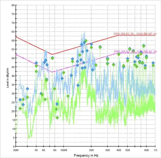
  • Product 1 is in a metal enclosure with a cut out for a TFT display and keypad, and several cables running out of the enclosure. The system is microcontroller based, with unshielded power, shielded CAN and shielded RS232 interfaces exiting the enclsoure. The problem seems to be coming from a 25MHz crystal that is driving the graphics controller and is leaking out from the cables and also from the front of the screen.

Product 01 scan

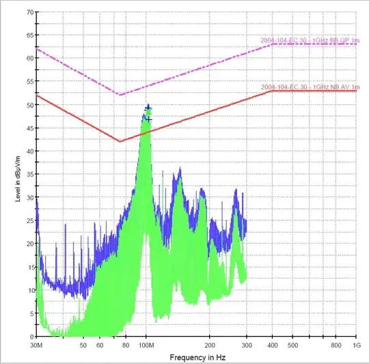
  • Product 2 is also in a metal enclosure but with a plastic window and cables running out. This system is microprocessor based (Linux) with unshielded power, shielded CAN and shielded RS232 interfaces exiting the enclosure. The problem in this cases appears to be stemming from the 3A, 5V switching power supply on the board (Lot's of 3kHz harmonics). There's also a lot of 45MHz harmonics stemming from the SD card. This product is open to design modifications

Product 02 scan

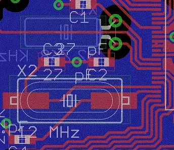
  • Product 3 is in a plastic enclosure with a large plastic window for indicators and cables running out. The system is microcontroller based with unshielded power, shielded CAN and unshielded GPIO interfaces exiting the enclosure. The problem seems to be stemming also from the same 3A , 5V switching power supply (same design as the previous item).

Product 03 scan

All three products are double layer boards.

What steps can I take and what solutions can I use to help reduce the radiated emissions of this existing design? What reference material (books, articles etc) can I use that discuss this topic?

Amr Bekhit
  • 1,278
  • 10
  • 24
  • 2
    I don't envy you. Fixing these problems after the design is frozen is not always possible, even with heroic efforts. This just serves to emphasize that it's far better to not generate the EMC in the first place than to try to suppress it later. – Dave Tweed Jan 15 '15 at 22:43
  • 3
    Unless you can charge by the hour :) – Some Hardware Guy Jan 15 '15 at 22:48
  • Are these 4 layer boards with reference planes (VCC, GND in the middle)? Or two layer? – Some Hardware Guy Jan 15 '15 at 22:49
  • 1
    @SomeHardwareGuy they're all 2 layer. – Amr Bekhit Jan 15 '15 at 23:02
  • I'd like to see a schematic and layout for the SMPS. Is the inductor shielded? – Matt Young Jan 15 '15 at 23:23
  • Note that you can add a link to the image in the description of it so that clicking on the images opens the higher res version. – PlasmaHH Jan 16 '15 at 09:50
  • 1
    @MattYoung the inductor is indeed shielded. I'm thinking of posting another question just on the SMPS, as the design is still open and it looks like it's going to be used in other designs as well. – Amr Bekhit Jan 16 '15 at 11:48

4 Answers4

5

There are a couple of general strategies you can consider:

  • Add shielding if there isn't already.

  • Close gaps in the shielding. Remember the radiating efficiency of an opening in the shield depends roughly on the largest dimension (a 4" x 0.001" seam radiates nearly as efficiently as a 4" x 4" hole), so concentrate on breaking up the longest seams with gaskets or other types of conductive materials.

  • Add EMI-absorbing material within the enclosure. This is usually a stop-gap to avoid changes in other parts of the design, but it's generally expensive and not necessarily very effective.

Beyond these general strategies, this kind of problem depends a lot on the details of your system and exactly what changes you can afford to make, so it's hard to be more specific about what you can do.

The Photon
  • 126,425
  • 3
  • 159
  • 304
  • 1
    Thanks for your suggestions. I've added more detail about my specific issues, in case that helps bring up more ideas. – Amr Bekhit Jan 15 '15 at 22:40
5

There are things you can do, photon has some nice tips above. Do you have the scans from the failure? Post one if you do. Get some emi probes I use these the loop one is the most useful. Borrow a spectrum analyzer or go to your testing house and use theirs (even if you aren't in a chamber). Now sniff out the source of your failure with the probes.

Start disabling things in your circuit or removing parts until you see the frequency you failed at go away. Gradually you will start to understand the source of the radiation, then you can start to deal with it with counter measures to see if it goes away.

You say you can't change the design, but you could probably swap components or maybe add a little resistor or ferrite bead here and there. Oh and don't underestimate the usefulness of using a spread spectrum clock source if your design can support it.

Some Hardware Guy
  • 15,815
  • 1
  • 31
  • 44
5

You're basically between a rock and a hard place.

The answer is shielding, both electric (e.g., sticky copper foil) and magnetic (e.g., ferrites around cables).

But pay attention to costs. If you can't respin the PCB, I'm guessing that you also can't retool the enclosures. But stopgap measures such as ferrites and copper foil are going to add significantly to your recurring costs, including the labor of installing them. It doesn't take long to get to the point where a respin would have been more cost-effective in the first place.

Dave Tweed
  • 168,369
  • 17
  • 228
  • 393
  • 1
    Thanks for your suggestions. I guess I'll probably see how far I can get with the band-aid fixes and then decide whether it's going to be worth it or not. – Amr Bekhit Jan 15 '15 at 23:23
5

One suggestion for the leaky windows would be to use a conductive mesh or coating gasketed to the case or case shield; this will suppress much of the RF coming out of them. As mentioned already, you'll want to use clamp-on ferrites around the cables to keep common-mode noise down (common-mode current measurements are a good way to find out if you have a problem there). Also, is the switching power supply in the second and third designs integrated into the same board as everything else, or is it a separate board? If it's the latter -- it may be worthwhile suggesting a quieter replacement for it.

Have a book, by the way.

EDIT: I didn't see you post the graphs until now -- while all I wrote above should be helpful, there's other things you can do as well, especially to the second product and it's pesky SD card slot. I'd suggest having the software devs underclock the SD card, and then making a hardware change to series resistors to the SD card lines near the IC that drives them -- these two changes, taken together, will reduce both the frequency of the noise (making it easier to shield and harder for the board to radiate) and its amplitude (by increasing the signal rise and fall times -- if you can use built-in slew rate control to do this, that's good too, for that matter).

ThreePhaseEel
  • 8,858
  • 4
  • 26
  • 41
  • 1
    Thanks for the useful suggestions and for the book recommendation! Regarding the SMPS, that's integrated on to the board. I am considering creating another question just focusing on that, though, because that's included in designs that are open to change at the moment. – Amr Bekhit Jan 15 '15 at 23:27
  • Good idea -- that SMPS sounds like it needs some tightening-up on the EMI front. – ThreePhaseEel Jan 15 '15 at 23:33
  • 1
    +1 for underclocking. I've been convinced that adding resistance near the output pin in series with each SD card line is a better approach than capacitors alone. Adding a capacitor alone to data lines often makes things worse. [Don't "despike" your signal lines, add a resistor instead.](http://techref.massmind.org/techref/electips.htm#series_resistor) – davidcary Jan 29 '16 at 15:18