3

I am building an inverting amplifier with an op-amp to attenuate a signal (ie: gain < 1) and I would like to be able to change the gain electronically by connecting multiple resistors to a switch or a multiplexer (as in this excellent answer.

It is possible to put this switch on either of the resistors in the inverting amplifier, making two possible circuits:

schematic

simulate this circuit – Schematic created using CircuitLab

Is there any reason to pick one of these circuits over the other? Are there any unexpected "gotchas" that I might be missing?

My gut tells me to go with circuit A because there is always feedback present - circuit B could have no feedback path while the switch changes positions.

Greg d'Eon
  • 3,807
  • 4
  • 24
  • 50
  • 1
    Have you considered using a programmable gain amplifier? – Vladimir Cravero Jan 13 '15 at 15:58
  • No, I hadn't heard of PGAs before. That sounds like another option as well. A quick Digikey search tells me that most of them are limited to 1, 2, 4, 8... V/V; I feel like that's a bit limiting, but definitely possible to design around – Greg d'Eon Jan 13 '15 at 16:02
  • 2
    It all depends on what you need to amplify. If you need precise gain control for, let's say, adapt an input signal to an ADC a PGA is the way to go. There also are digital volume controllers, you can talk to them via i2c ora via two buttons and change the attenuation from input to output, assuming your signal frequency is low. Not sure volume controllers work with DC though. – Vladimir Cravero Jan 13 '15 at 16:08
  • One way to deal with the open switch in B is to always have the largest FB resistor connected, and use the switch to put smaller R's in parallel. Another option is a switched voltage divider and unity gain buffer. (Switch at ground ala- Spehro below.) – George Herold Jan 13 '15 at 16:29
  • @GeorgeHerold: Your first suggestion is ala-Andy below :) I think that's what I'm going to do. – Greg d'Eon Jan 13 '15 at 16:41

7 Answers7

12

There are probably better switchable gain op-amp configurations if you use a non-inverting gain topology. For a start, the impedances around the feedback and grounding resistors can be much lower and hence the leakage currents produced by the analogue switch produce significantly smaller offset voltage errors. One further advantage is that the analogue switch can become a simple JFET if you choose to change gain by grounding different values of resistors: -

enter image description here

You can have several versions of Rg connected to ground by JFETs or analogue switches. Note that in this configuration, resistor selection (by switches) does not impart any changing conditions on the input impedance of the amplifier.

If you insist that the inverting topology is used I would recommend the switching be in the feedback loop and you don't need to worry about breaking the loop - your maximum gain would be set by a permanently connected resistor of the highest value and your switch(es) would connect more parallel resistors in order to lower the gain - input impedance into the circuit is unaffected by this method.

Andy aka
  • 434,556
  • 28
  • 351
  • 777
  • Aha - I should have mentioned that I'm actually using this as an attenuator (gain < 1) so a non-inverting amp doesn't work for me. This answers the question that I asked, though. The last paragraph is a good idea. – Greg d'Eon Jan 13 '15 at 15:30
  • 4
    You can still use a non-inverting configuration for gains less than unity - just add a basic attenuator to give you the lowest gain and then use gains>1 for the higher gains. – Andy aka Jan 13 '15 at 15:33
7

Attenuation is pretty simple: use a potentiometer. If the output resistance isn't acceptable, then you can follow that with a buffer:

schematic

simulate this circuit – Schematic created using CircuitLab

There are not a lot of gotchas with this approach: the op-amps you have are probably unity gain stable (check the datasheet).

Of course the problem is how to adjust the potentiometer without turning a knob, but there's a solution for that too: a "digital potentiometer". You can find hundreds of them from any parts vendor with just about any digital interface you want.

Phil Frost
  • 56,804
  • 17
  • 141
  • 262
  • Some more thinking out loud: in my case (where I want to switch between discrete attenuation values), the potentiometer could be replaced with several voltage dividers on a switch/relay/multiplexer. This seems very simple. – Greg d'Eon Jan 13 '15 at 17:31
  • 1
    @Kynit Yes. If you needs are even simpler, the "multiplexer" could even be transistors with their emitters/drains connected to ground: just ground the resistor(s) you want by switching on the corresponding transistors. – Phil Frost Jan 13 '15 at 21:20
  • This is correct because an amplifier should have only one operating point. Otherwise, you have to make the amplifier stable in multiple conditions with only one choice of capacitive feedback! – Cuadue Jan 13 '15 at 21:30
5

The top circuit is better in some ways, but I would prefer to see the switch right on the op-amp input and the resistors on the other side, which will greatly reduce the nonlinearity (distortion). If the input voltage can exceed the mux power supply range you have to be careful about the 'disconnected' resistors conducting current through the chip's internal protection networks and causing errors.

The bottom circuit could be an advantage if you need to deal with relatively high voltages (say 100V) at the input.

In both cases, the switch resistance and leakage will enter into the error budget, so take care if this is intended to be a precision circuit.

Edit: To expand on the nonlinearity issue:

There are two error terms- the constant switch resistance (it varies unit-to-unit and with temperature and supply voltage, but let's ignore those), and there is a variable component that changes with the switch voltage with respect to ground or supply rails. Connecting the switch at a virtual ground point means that the variation due to voltage is minimized (both input voltage and output voltage are near to 0V if switch resistance is low in comparison to the resistors, which it should be). Connecting it on the other side of the resistors maximizes the voltage change (it will follow the inputs directly) and so maximizes the distortion.

Spehro Pefhany
  • 376,485
  • 21
  • 320
  • 842
  • Can you explain the non-linearity reduction in a bit more detail? I think you're proposing that the switch and the resistors switch places, and I don't understand how that would act differently. – Greg d'Eon Jan 13 '15 at 15:58
  • 1
    See edit above, and look at the datasheets for typical analog switches. – Spehro Pefhany Jan 13 '15 at 16:12
  • Perfect - that's very clear, and the datasheet I already had open agrees with you. – Greg d'Eon Jan 13 '15 at 16:13
  • 1
    (thinking out loud for future readers) This means that circuit B is already optimal for an analog switch. Swapping the resistors with the switch would maximize the distortion in exactly the same way Spehro described here. – Greg d'Eon Jan 13 '15 at 16:18
2

Neither of those are a good idea as the majority of switches are 'break before make' so for an instant in each of those cases, the path with be an open circuit. Very bad for the feedback resistor as your gain will go way up and it will likely slap against the rail and/or oscillate. Instead I would suggest changing the resistance by adding another resistor in parallel. So for a 2:1 change, if the Rf was a 100k resistor, then adding another 100k in parallel would result in 50k.

1

There are two kinds of designs of switched-gain amplifiers: those that have significant signal currents flowing through the switch, and those that don't. Off-the-shelf analog switches, such as the DG family from Intersil, etc., have the following drawbacks:

  1. Switch resistance depends on the absolute voltage of the signal - this modulates the gain of your circuit, and adds distortion.

  2. Switch resistance can be at best compensated by a factor of 10 by using another switch on the same die as a reference. The switches' on resistance typically matches within 10% and temperature tracking should be similar on one die.

So, the solution is to avoid all that. This lets you get away with using potentially much cheaper switches, too.

schematic

simulate this circuit – Schematic created using CircuitLab

This helps as follows:

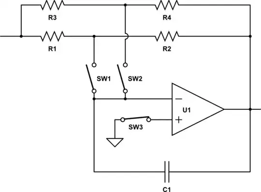
  1. The op amp inputs have high impedance, so that "no" current flows through the switch.

  2. The switch does carry the op-amp's bias/offset currents. If you want to compensate for it, leave the SW3 from the same package in series with the positive input. That switch will be closed at all times. If the op-amp has very low offset current, you can delete SW3. Some op-amps have decorrelated "offset" currents and for lowest noise should not use unnecessary source resistance on the "other" input. The datasheet would indicate that.

  3. The switches all "see" the constant voltage present at the positive input of the op-amp, and thus their resistance isn't modulated by the signal.

Of course, nothing is free. The op-amp's open-loop gain is reduced, since it sees lower load resistance on the output -- all the gain dividers load the output in parallel.

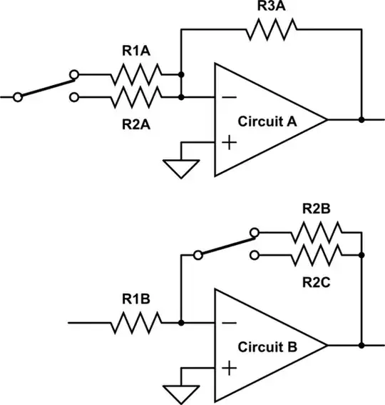
Judicious selection of U1 allows to keep the performance satisfactory with multiple switches. If you need more gains, factor out common integers and split the gain between two stages. This would be necessary to maintain the bandwidth of the system anyway, or to keep the noise in check by not having to have excessive GBW at low gains.

C1 is generally a good idea, but it should be selected so that its effects are far away from the passband. You don't want the variable resistance of the switch distorting your signal.

0

The transfer ratio of the inverting configuration is -R2/R1; so it depends linearly on R2 and hyperbolically on R1. This is another argument in favor of the second inverting circuit (with a variable R2).

Another source of error is the varying voltage drop across the switchable resistor due to the op-amp input bias current.

If the analog switches connected to the summing point of the inverting configuration have some input current (like the base current of the old BJT switches), it will enter the summing point and will be added to the input current (another error).

R-2R ladder (multiplying DAC with current output, e.g. the old AD 7533) is a suitable element for implementing a digitally-controlled resistor R1 (R2), and accordingly, an amplifier with a programmable gain.

Circuit fantasist
  • 13,593
  • 1
  • 17
  • 48
  • I'm confused about your first two points. Why do you think it's worse to change the component with a hyperbolic relationship? Why is the input bias current significant compared to the regular input current? I'm not sure what typical leakage currents are, but the switch I'm looking at says 1 nA max. Not a big deal, but could be important for lower-cost parts. – Greg d'Eon Jan 13 '15 at 16:56
  • I said it is better (suitable) to change the element with a linear relationship (R2). Really, the impact of the input bias current of nowadays op-amps is negligible (if you keep the equivalent resistance relatively low); the same applies to the leakage currents of the switches. So my remarks are of a general nature. – Circuit fantasist Jan 13 '15 at 17:05
  • "It is better (suitable) to change... R2." Yes, this repeats what your answer says. Why is it better? – Greg d'Eon Jan 13 '15 at 17:07
  • Maybe because the transfer ratio will depend linearly on R2... and the circuit input resistance will stay constant... BTW it is possible to switch the resistors of a T-network connected in the place of R2 (it is not suitable for your case where R2 < R1). – Circuit fantasist Jan 13 '15 at 17:17
  • No, I still don't get why linearity is important for discrete choices of resistors. Constant input impedance is a good thing to have, though. – Greg d'Eon Jan 13 '15 at 17:19
  • It is not so important... but the ratio between the particular resistances will not be significant... – Circuit fantasist Jan 13 '15 at 17:25
0

From all answers above I can only agree that the voted answer is best because switches or Fet's are almost linear due to their ground level.

But there's one issue that has not been discussed above: if switches are in the feedback loop near opamp input, they have to be layed out on a PCB and they are directly coupled to the most sensitive pins of the opamp: the input pins. From experience, this leads to very sensitive circuits that pick up noise easily.

This issue is non-existent in the solution provided by switching Rg to ground in non-inverting topologies.

gommer
  • 1,023
  • 6
  • 17
  • Welcome to EE.SE. Note that "all the answers above" is almost meanlingless on StackExchange as posts move up and down with votes and user sorting preferences. – Transistor Jan 22 '18 at 20:16
  • I understand, at least I've corrected for more meaningful references. – gommer Jan 23 '18 at 08:43