2

enter image description here

Consider this circuit, this is a gyrator and acts like an inductor. Why when we analysis this circuit do we use assume negative feedback (i.e. the voltage at each input is the same). I thought that we only use negative feedback when the output is connected to only the inverting input, however in this circuit, we have both positive and negative feedback, as the output is connected to both the negative and positive inputs. So why do we only assume negative feedback takes place?

  • 3
    There does not have to be only negative feedback, only more negative than positive. – Spehro Pefhany Jan 12 '15 at 19:51
  • @SpehroPefhany how do we know if there is more negative or positive? – Quantum spaghettification Jan 12 '15 at 20:18
  • 1
    Look at the circuit - voltage divider with more net negative fb. – Spehro Pefhany Jan 12 '15 at 20:35
  • @SpehroPefhany more negative since the output of the op-amp has a larger effect on V- to V+?? – Quantum spaghettification Jan 12 '15 at 20:38
  • The output of a given op-amp has more effect on its inverting input than on its non-inverting input. – Spehro Pefhany Jan 12 '15 at 20:50
  • On the matter of both positive and negative feedback, there's [another question here on SE on that](http://electronics.stackexchange.com/questions/112472/how-are-positive-and-negative-feedback-of-opamps-so-different-how-to-analyse-a), which unfortunately doesn't have very good answers... actually has one with a mistaken formula but still upvoted. Stay tuned as the saying goes. – Fizz Jan 12 '15 at 22:36

4 Answers4

5

"So why do we only assume negative feedback takes place"

It is not correct that "we assume negative feedback" only. Who say this?

The shown two-opamp circuit (introduced by A. Antoniou) can be interpreted as a combination of two "Negative Impedance Converter (NIC)" circuits. There are two basic NIC types (current-inversion - INIC, and voltage-inversion - VNIC) and both exhibit a negative input impedance. However, a stable combination results if we replace the grounded output resistor of the first NIC unit (INIC) with the negative input impedance of the second NIC unit (VNIC).

This forms already a circuit called "Generalized Impedance Converter GIC". However, this form has some disadvantages - and therefore a modification is used which is known as Antonious GIC circuit (as shown in the question). It is easy to show that this alternative has the best properties of all possible modifications - as far as influence of real opamp parameters is concerned. This form can be derived from the simple NIC combination exchanging some opamp input nodes which are (for ideal opamps) at the same potential.

This GIC is extensively used in active filter realizations as an "active inductor" and/or as a "Frequency-Dependent Negative Resistor (FDNR)".

Circuit fantasist
  • 13,593
  • 1
  • 17
  • 48
LvW
  • 24,857
  • 2
  • 23
  • 52
  • I'm not blaming you for not including formulas/derivations here (given what the question asks), but if anybody wants to read those see [these slides](http://www.eece.cu.edu.eg/~maboudina/teachingmat/ELC302Spring2013/ELC302S13_Lec9_ActiveL_FDNR_Leapfrog.pdf). The gyrator and Antoniou's GIC are covered on slides 6-7 after some prerequisites. – Fizz Jan 12 '15 at 22:41
  • Nice slides - in particular, because they show Riodan´s realization and they introduce Bruton`s transformation. – LvW Jan 13 '15 at 09:14
3

This "devil" circuit reminds me of some of Antoniou's GIC circuits. I spent a lot of efforts to figure out their secrets in this ResearchGate dialogue. Maybe it will help.

First Antoniou's GIC circuit

As @LFW has noted above, the grounded load resistor of the first NIC (INIC) is replaced by another NIC (VNIC). So, to understand circuit, we need to reveal: first, the role of the second NIC B (VNIC); next, the role of the grounded load resistor of the first NIC A (INIC).

Second Antoniou's GIC circuit

Well, let's begin with considering the second NIC (VNIC) assuming that Z5 is a capacitor. This circuit acts as a negative inductor since the op-amp adds a voltage to the previous circuit (connected to its inverting input) equal to the voltage drop across the grounded resistor Z6... and this voltage represents the voltage drop across an inductor (this is a property of the simple RC circuit where the "complementary" voltage drop across the resistor behaves through time as the voltage drop across an inductor)...

Now about the role of the grounded load resistor Z6 in the VNIC... It acts as an "original" for creation of a "voltage-inverted copy". Briefly speaking about the VNIC operation, the op-amp keeps up the current through the "original element" equal to current through the input source, and "inserts" (adds) a reverse voltage into the circuit equal to the voltage across the "original element". To understand how the op-amp does this magic, think of the VNIC circuit (excluding only the op-amp) as of some kind of a balanced Wheatstone bridge with a varying supply voltage. See more about the topic in this RG question dedicated to NICs and the similar Wikibooks story.

Now about the role of the grounded load resistor of the first NIC (INIC).

enter image description here

It acts as an "original" for creation of a "current-inverted copy": if it has a positive impedance (the usual case), the "copy" will have a negative impedance adn v.v., if it has a negative impedance (our case), the "copy" will have a positive impedance... This op-amp circuit does this "magic":) by inverting the current through the input voltage source; thus the name "negative impedance converter with current inversion" (INIC). In brief, the op-amp keeps up a voltage drop across the "original element" equal to the voltage of the input source, and "pushes" a reverse current through the input source equal to the current through the "original element". To understand how the op-amp does this magic, think of the INIC circuit (excluding only the op-amp) again as of some kind of a balanced Wheatstone bridge with a varying supply voltage. As a result, the whole circuit acts as an "inverted original element"... and, for example, if the "original" is a positive resistor, the circuit will be a negative resistor.

Finally, if we look again at the exotic second Antoniou's circuit, we can see that a negative inductor (the second NIC) is connected in the place of the grounded load resistor... so its negative inductance is converted into a positive inductance... thus the whole GIC circuit acts as a "positive inductor"...So, in this arrangement, the generalized impedance converter (GIC) is an "inverted negative inductor"... or a "double inverted inductor"... what gives a "positive virtual inductor"... or simply an inductor:)... So, we can explain this circuit in a 3-step "scenario:

  1. Take a "real capacitor"
  2. By using a VNIC, swap the current through and voltage across the capacitor thus obtaining a "virtual negative inductor"
  3. By using an INIC, invert the "virtual negative inductor" (more precisely, its current or impedance) thus obtaining a "positive virtual inductor"...

Simply, we can say it in more striking way: "By one swap and next two consecutive negations, the Antoniou's GIC circuit converts a real capacitor into a virtual inductor."

We can add also that while the single NIC is usually a "positive-to-negative impedance converter" while this compound GIC is a "positive-to-positive impedance converter"...


It now remains only to see the connection between this demystified circuit solution and the circuit in the question. It seems there is such a connection since:

  • At least, they both contain the same elements (four resistors, one capacitor and two op-amps).
  • We can see the differentiating CR (Z5,Z6) circuit that produces the same voltage drop across the resistor as in the case of an inductor
  • They both contain a resistor R2 connected between the input source and the circuit (it is used by the circuit to make an impact on the input source so that to simulate an inductor).
  • Now let's try to do the most difficult - to see the two NICs; let's begin with the VNIC (the negative inductor). IMO it is implemented by the upper left op-amp with the differentiating circuit (Z5,Z6) connected as a positive feedback, and the resistor Z4 (in combination with the INIC below) connected as a negative feedback. Note the positive feedback is not simply connected to the non-inverting input; it is closed through the other (lower right) op-amp.
  • Now only remains to see where the INIC (the negative-inductance inverter) is; it should be composed of the remaining elements. So it seems Z2 is connected as a positive feedback, and Z3 (in combination with the VNIC above) - as a negative feedback. Note again the positive feedback is not simply connected to the non-inverting input; it is closed through the other (upper left) op-amp.
Circuit fantasist
  • 13,593
  • 1
  • 17
  • 48
  • In the case of my circuit, I cannot see why get something acting like an inductor? In assuming that we have negative feedback the voltage drop over the last resistor is Vin and the current through it is simple Iin so why is not the total impedance not the value of the last resistor=Vin/Iin? – Quantum spaghettification Jan 13 '15 at 09:07
  • Joseph - it`s not so simple. Let`s take as an example the INIC as shown in this reply (above). The voltage at the noninv. input nearly equals the voltage at the inv. input. That´s OK. But we speak about the input impedance as seen at the non-inv. input - and where does the resulting current go? Through the feedback resistor R. Hence, not only R1 is involved (as you might think). OK? – LvW Jan 13 '15 at 14:21
0

Oh my God! I can't believe it but this morning I still managed to find a simple and powerful explanation of this intricate circuit... and it is based only on the humble op-amp Golden rules! I only hope I could explain it in the same simple way...

The general idea is to simulate (emulate, make virtual) an inductor by the dual capacitor... or more precisely, only to imitate the inductor's time behavior with an active RC circuit.

To implement this idea, we have to swap the current and voltage in a capacitor. We can do it if, in an RC network (R4,C here) driven by the input source, we do the following:

  • copy the voltage drop (Vc) across the capacitor and convert it into an input current (Iin) of the simulating circuit
  • copy the voltage drop (VR4) across the resistor and impose it on the input of the simulating circuit.

In Antoniou's genius circuit, we can see two interacting op-amp NFB systems that keep up equal voltages at the three points A, B and C (VA = VB = VC)... and so zero differences (voltages) between them (VA - VB = VB - VC = VA - VC = 0). As a result:

  • VA (the input voltage of the simulated inductor) is equal to VR4 (that is proportional to the current through the initial capacitor); so, the voltage across the virtual inductor is proportional to the current through the initial capacitor
  • VR1 (that sets the input current of the simulated inductor) is equal to VC (the voltage across the initial capacitor) since the same current flows through R2 = R3 -> VR2 = VR3 -> VR1 = VC; so, the current through the virtual inductor is proportional to the voltage across the initial capacitor.

It would be very interesting (at least, for me) to draw the currents (in a form of closed loops) and voltages (as bars) with their directions and signs.

Enumerated GIC

A more conventional way to implement this idea is by using a fixed gain amplifier (follower). See for example this Wikipedia discussion and old article where the circuit is presented as a bridge.

Circuit fantasist
  • 13,593
  • 1
  • 17
  • 48
0

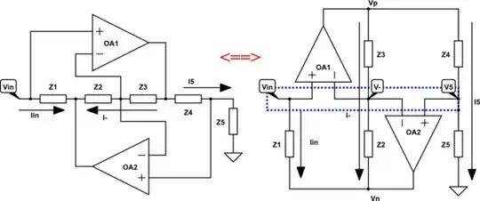
I like to redraw the gyrator circuit to make the current arrows flow top-to-bottom. I find it's more intuitive and easier to understand what's going on in the top-down flow:

schematic

simulate this circuit – Schematic created using CircuitLab

This way, it's more apparent that the op amps are providing sort of "virtual floating rails" for the 3 current flows in the system (the voltages \$V_p\$ supplied by \$\text{OA}_1\$, and \$V_n\$ supplied by \$\text{OA}_2\$).

It also helps when visualizing the virtual equivalence of the op amps' input nodes (assuming they are operating in negative feedback). Is that assumption correct?

Let's start by holding \$V_{in} = V_- = V_5 = 0\$. That means the currents are 0, and both \$V_p\$ and \$V_n = 0\$.

Now if \$V_{in}\$ were to go ever-so-slightly positive, then \$\text{OA}_1\$ see a positive voltage difference between its noninverting and inverting inputs (\$V_{in}\$ and \$V_-\$), so it would drive \$V_p\$ high, by its open-loop gain (typically, at least \$10^5\$). That imputes current \$I_- = (V_p - V_-)/Z_3\$, which flows through \$Z_2\$, driving \$V_n\$ below \$V_-\$.

But (relatively) high \$V_p\$ also drives current \$I_5\$, raising the voltage at \$V_5\$, because \$Z_5\$ is grounded. As \$V_5\$ increases such that \$V_5 > V_-\$, then \$OA_2\$ drives \$V_n\$ positive, reducing the voltage drops across \$Z_3\$ and \$Z_2\$. This in turn implies a raising \$V_-\$, reducing the difference across \$OA_2\$'s inputs, and thus lowering \$V_n\$.

This cycle of mutually-stabilizing "virtual rails" output by the op amps results in the virtual equality of \$V_{in} = V_- = V_5\$.

A similar analysis at each node, assuming any (reasonable) initial voltages, will show the system stabilizes to \$V_{in} = V_- = V_5\$, meaning the op amps are both operating in mutual negative feedback.

This arrangement also helps to show the amplitude limits of the system. Just using all real, equivalent impedances (i.e., resistors), then \$V_p = 2\,V_{in}\$, and \$V_n = 0\$. If the supply voltages \$+V_{cc}, -V_{ee}\$ (or \$+V_{dd}, -V_{ss}\$) are, say, \$\pm15\,\text{V}\$, then \$V_{in}\$ must stay within \$\pm7.5\,\text{V}\$ to maintain closed-loop operation. Of course, with non-equivalent impedance values, you can't always assume \$V_p = 2\,V_{in}\$ or \$V_n = 0\$ (the \$(Z_3,Z_2)\$ and \$(Z_4,Z_5)\$ resistor ladders' ratios determine the ranges of \$V_p\$ and \$V_n\$ with respect to \$V_{in}\$).

scottbb
  • 107
  • 4