2

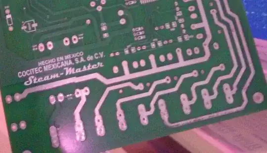
How can I design a PCB in order for it to have this kind of PCB Tinning finish?

I do know this decreases the resistance of the tracks and increases the amount of current it can handle however

Do I need to leave the solder mask below and do it by hand?

Do I need to remove the solder mask ?

Can this process can actually be done at the fab house?

Edit 1-----------------------------------------------------------

Now an interesting question, Is there any kind of design rule to follow using this HASL finish? , I mean the rule its 40mils per Amp however if I get a 40mils HASL finish track, can I actually put 2 Amps on that?, if the answer is yes, isn't the solder conductivity lower than the copper itself?

enter image description here

Roh
  • 4,598
  • 6
  • 41
  • 86
GoatZero
  • 1,527
  • 4
  • 28
  • 44

4 Answers4

9

While DrFriedParts provided an answer to the question you asked, I feel I ought to respond to your premise, instead. Specifically, "i do know this decreases the resistance of the tracks and increases the amount of current it can handle", while technically true, is not a reason to specify HASL. Let us consider. A 1 oz copper trace has a thickness of 1.37 mils, and a bulk resistivity of ~0.017 uohm-meter. A typical HASL layer is 0.1 to 0.3 mils, and the bulk resistivity is ~0.17 uohm-meter. So HASL will add about 15% to the cross-sectional area of the trace, but with a resistivity about 10 times greater than the trace provides. The result of this is that the resistance of the trace is reduced less than 2%, and the current-carrying capacity is increased by the same amount.

Trust me, if you absolutely must have the extra 2% you are doomed.

HASL is a perfectly reasonable finish, but is does not do anything noticeable to your current-carrying capacity.

WhatRoughBeast
  • 59,978
  • 2
  • 37
  • 97
  • so then when should HASL be used then if it barelly increases the carring current capabilities? – GoatZero Dec 22 '14 at 22:57
  • 2
    You use it whenever you want easy soldering to your traces, particularly if you're going to store the PCBs for any length of time before assembly. You also use it if the boards will not be in a corrosive environment and you want to keep costs down. – WhatRoughBeast Dec 22 '14 at 23:29
  • thats sounds like a solder pad HASL but i was thinking about the track HASL, usually the track comes covered by the solder mask bt if i decide to have it covered by HASL then there must be a reason, i was thinking it could be used to increase the current capacity by huge amounts but according to your response its not posible, however the tracks in the picture i added have no soldermask and are covered in solder, so there must be a reason to do this – GoatZero Dec 22 '14 at 23:45
  • @GZeromostro One possible reason is that heat will dissipate faster from traces that don't have soldermask. – bitsmack Dec 23 '14 at 00:30
6

When solder is added on top of the traces in order to increase the current carrying capacity, it's usually done during wave soldering 1.

The solder mask is designed with windows on top of the traces. When the board runs through the solder wave, the solder sticks to exposed copper.

enter image description here (source of picture)

Notice that the board in the O.P. is unpopulated. It's possible that it was designed for wave soldering, and it just haven't been through the wave yet. After it goes through the wave, more solder will stick to the exposed traces.

Probably, a similar effect can be achieved with solder paste and IR reflow. You'd have to consider carefully the shape of the solder paste stencil.

The purpose of HASL is to make the solder layer as flat as possible. This is to prevent misalignment of SMT components. @WhatRoughBeast has already mentioned that the layer of solder after HASL is comparatively thin. On the other hand, to decrease the resistance, it's desirable that solder is as thick as possible. Different objectives.

1 I'm surprised that nobody have mentioned it yet.

Nick Alexeev
  • 37,739
  • 17
  • 97
  • 230
  • The OP's photo is not wave soldered, but you may be right that it was designed for a selective solder fixture + wave. You can see the exposed areas are tinned and there are SMT pads. It's possible that the designer just didn't realize how ineffective plating is with respect to a current handling increase or perhaps took the "better than nothing/can't hurt" approach. – DrFriedParts Dec 23 '14 at 21:57
  • 1
    @DrFriedParts Most of the components on the board in the O.P. are throughole. There are only few SMTs, and they are not particularly small (0805, or 1206 by eyeball). As you probably know, it's possible to wave-solder SMT components too. Glue dots hold the SMT component. This glue dot approach is fairly common and cost-effective. (The glue dot is usually reddish-brown in color, sometimes it squishes from under the SMT component and you can see it in the finished board.) – Nick Alexeev Dec 23 '14 at 22:09
  • Absolutely. I'm not disagreeing (in fact, I up-voted this), just musing on why it's this way... personally, I'm in the designer didn't know what s/he was doing and just monkey-see-monkey-do copied the look-and-feel of a competitor's PCB. You can see many wide tracks under solder mask and many left exposed seemingly at random. Whatever logic led to the exposed tracks it should either apply to all or none. – DrFriedParts Dec 24 '14 at 02:37
3

HASL, and it's real common

This finish is often called HASL (Hot-air solder leveling). It works like this:

enter image description here

This is a vertical hot-air solder leveling machine. Solder is applied to the board (in areas that are not masked off) and then it is reflowed under constant diffuse positive air pressure. Basically, the solder is turned "wet" (flowable) and then blow down to counter the natural surface tension which will give it an arch-shaped profile otherwise. The hot air is gradually reduced in temperature (while maintaining pressure and flow-rate) allowing the solder to solidify in its blown-down (flat) shape.

Design-in

It's simple. Just tell your fabricator you want a HASL finish (it's usually the cheapest finish they provide) and leave your tracks exposed in your solder-mask artwork.

DrFriedParts
  • 12,482
  • 36
  • 54
2

Dave Jones from the EEVblog posted an interesting video on this. https://www.youtube.com/watch?v=L9q5vwCESEQ

  • 1
    Welcome to Stack Exchange. This is a [questions and answers site](http://stackoverflow.com/about), not a link collection. Please include relevant content in your answer, not just a link to where the content may be. The link is nice to have in addition for reference or for further information. For more tips, see [How to answer](http://stackoverflow.com/questions/how-to-answer). – Nick Alexeev Dec 23 '14 at 03:39