1

I'm trying to create a dummy load circuit, but it was limiting itself around 1.7 A, so I built this circuit. V1 is 0 - 5 V via a potentiometer, and V2 is a 5 V / 3 A power supply.

schematic

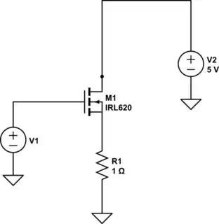
simulate this circuit – Schematic created using CircuitLab

When I increase the voltage Vgs, even up to 5 V, the current through the power supply (measured with a multimeter) limits itself to around 1.7 A. If I remove the 1 Ohm resistor, the current is not limited at all, and keeps rising.

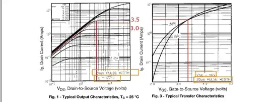
I have looked at these two diagrams on the datasheet of the MOSFET, but can't seem to figure out why the current limits itself due to the resistor:

enter image description here enter image description here

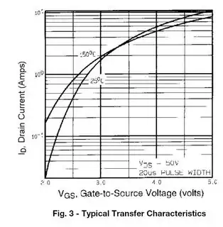
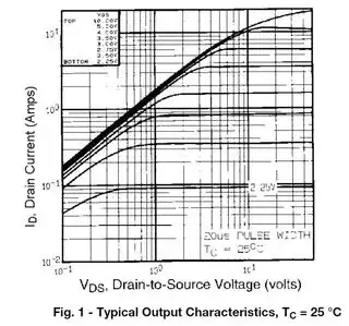
I wanted a 3A current through the power supply / MOSFET / resistor, so I looked at figure 3. For a 3 A current, Vgs needs to be ~3.4 V. At 3 A, there will be a 3 V drop across R1, so Vds will be 2 V. Then I looked at Fig 1, and at Vds = 2 V, it should be able to have an Id of 3 A, given that Vgs = 3.4 V.

So why can't I get 3 A out of this circuit?

Null
  • 7,448
  • 17
  • 36
  • 48
tgun926
  • 2,726
  • 12
  • 36
  • 59
  • I think the key words here are "typical" and "at 25 degrees C" – W5VO Dec 22 '14 at 05:54
  • R1 causes Vg to need to be greater than Vgs, based on how much current is flowing through it, and simultaneously reduces Vds. – Ignacio Vazquez-Abrams Dec 22 '14 at 05:57
  • @W5VO So my calculations are correct? I didn't test at Vgs = 3.4V though, even at 5V it limited to 1.7A. Further, the mosfet is on a big heatsink. – tgun926 Dec 22 '14 at 05:58
  • @IgnacioVazquez-Abrams What's the difference between Vg and Vgs? – tgun926 Dec 22 '14 at 06:00
  • Vg is the voltage you apply to the gate referenced to ground, and Vgs is the voltage difference across the transistor. – Ignacio Vazquez-Abrams Dec 22 '14 at 06:01
  • @IgnacioVazquez-Abrams: Vg is the voltage between the gate and ground, Vgs is the voltage between the gate and the source, and Vds is the voltage across the transistor. That is, from drain to source. – EM Fields Dec 22 '14 at 06:47

6 Answers6

3

What you observe is very well described by calculating the voltage drops across the various components and then looking up the results on the data sheet graphs that you have provided.

The three key factors are

  • What is the FET Rdson value at the operating point that you observe, what is the consequent Vds drop and what affect does this have.

  • What is the drop across R1 at the observed current, what is the resultant Vs and what affect does this have?.

  • Do the data sheet "typical" parameters match what you expect to see in the steady state in your application?
    Clue: Guess.

You are a victim of a number of things which add to aifd Murphy. The FET has a nastily high Rdson - exact value uncertain but if 1 Ohm as it may be then you have extra resistance combatting current flow.
As W5Vo said - the results are 'typical' - and they then add weasel word fine print to the graphs to define typical.

See the orange boxes.
The "weasel words" 20 uS pulse width is to allow the die to heat minimally and cool again between pulses. Rdson can be double in some cases with some FETs at full steady state temperature. In your case fig 4 shows Rdson with die temperature.

You showed fig 1 which is at 25 C.
Now look at fig 2 which is at 150 C. At about 2V Vds (higher Rdson due to hotter die) and 3.3V Vgs the operating point lies above the available plots. You can only get back onto the graph with higher Vgs or lower Vds (so lower current). That's at 150 C. Your reality lies between the two curves and depends mainly on your Rdson which depends on the effective thermal Rja which depends on your heat sink.

Note the Vds in Fig3. **50 Volts ** !!!!!!!!!!!!!!!!!!!!
Fig 1 is at 25C - if ambient is 25C and you have 1.7A at 1 Ohm = 1.7 Watts the die temperature will be highly dependant on heat sink. Infinite sink - Tjc = 2.5C/W - rise about 4 degrees C. Cool!
Open air no sink Tja = 62 C/W - rise about 100 C+ - and Rdson will rise so dissipation will rise so ... . Touch not the FET bot a glove!

enter image description here

enter image description here

At 1.7A Ids, V_R1 = 1.7A.
V1 = 5V so Vgs = 3.3V.

Recalc, rinse, repeat.
Asymptote is liable to be about what you see.

enter image description here

Russell McMahon
  • 147,325
  • 18
  • 210
  • 386
  • I've been trying to understand this for a few hours now, and I'm still stuck regarding the operating point business - For a given Vds, why is the drain current higher for the higher junction temperature? Shouldn't Rdson be higher, hence a lower current (referring to Fig 1 vs. 2) – tgun926 Dec 23 '14 at 06:24
  • @tgun926 Exact answer to where it will end up is unknown. Too many interacting variables. I tried to provide a guide to the various things that may "confound" a static answer. I won't at this stage look at what you are pointing out - which may well be correct (or not) depending on what other assumption are made. ||| Turn on. Current flows. Vgs falls s current rises due to Vr1 rising with current so Rdson rises with lowering Vgs. I^2.Rdson heats FET. Rdson rises with temperature decreasing current. Vgs rises with decreasing current lowering Rdson... . A stable point is reached. .... – Russell McMahon Dec 23 '14 at 09:38
  • ... If you posot the stable point correctly and work things out they all ba;ance. If you guess eg Ids too high the calculation yields a lpower value and you try again. | Factor in "typical values", data given at eg 25C or Vds - 50-V or pulsed current and data sheet becomes just a guide. | A valuable lesson is that a crrent limiting circuit that depends on Vgs and Rdson is going to be a very variable and approximate one and if you want precision you use external control. | Main thing you get wih a very cheap opamp added is v high loop gain so accurate comparison with a reference and ... – Russell McMahon Dec 23 '14 at 09:42
  • ... operating point not dependant on power device characteristics. eg use lm324/4 IR lm358/2 (both are same amp) set R1 = say 0./1 Ohm and derive a 0.3V reference. Opamp drives FET. OA- to R1 top. OA+ to 0.3V ref. A close to "perfect" 3A max supply (if FET used allows 3A with what voltage OA will supply.) – Russell McMahon Dec 23 '14 at 09:44
2

The current through the MOSFET is governed by the Gate-to-Source voltage, not the Gate-to-Ground voltage.

With 1.7 Amp through the FET, there will be 1.7 volts across R1, making the Gate to Source voltage 1.7 volts less than the V1 voltage.

Peter Bennett
  • 57,014
  • 1
  • 48
  • 127
  • He's understood that - see the end of his question. What he is trying to do is build a current limiter by using this feature to place the FET at an operating point of his choice. – Russell McMahon Dec 22 '14 at 06:55
2

For a 3A current, Vgs needs to be ~ 3.4V.

...

So why can't I get 3A out of this circuit?

For the circuit as drawn, write the equation for the gate-source voltage :

$$V_{GS} = V_G - V_S = V_G - I_D\cdot 1\mathrm \Omega $$

For \$I_D = 3 \mathrm A\$, the equation is

$$V_{GS} = V_G - 3\mathrm V$$

But you've stipulated that

$$V_{G,max} = 5V$$

So, with the maximum voltage applied to the gate and \$I_D = 3 \mathrm A\$, we have

$$V_{GS,3\mathrm A} = 2V\mathrm \;<\; 3.4\mathrm V$$

In other words, a contradiction.

Thus, with \$V_G = 5\mathrm V\$, the current must be less than \$3\mathrm A\$.

Alfred Centauri
  • 26,502
  • 1
  • 25
  • 63
1

I suspect that the problem is the on resistance of the transistor. According to the datasheet, RDSon can approach 1 ohm under fairly normal circumstances. That limits you to 2.5A (5V / 2ohms) . If the temperature increases (which it will, even with a heat sink), the RDSon goes up some more. 5V might not be enough for V2. I bet you'd get better results with a 10V supply.

Adam Haun
  • 21,331
  • 4
  • 50
  • 91
1

The problem is that since the drain-to-source resistance (Rds) varies inversely with the gate-to-source voltage (Vgs), as soon as Vgs increases to the point where Rds starts falling and allowing power supply current through the transistor, that current also flows through the external source resistor.

That current then causes a voltage drop across the source resistor which increases the voltage on the source, causing the slope of Vgs to diminish somewhat, limiting the change in current through the transistor as the gate's source voltage increases.

That's shown graphically, below, where the red trace shows an independent 0 to 5 volt increase in the gate voltage, Vg, the green trace shows Vgs changing because of the change in voltage across R1 as the current through R1 changes, and the yellow trace shows the change in current through R1 as Vg and Vgs change.

The LTspice file is here if you want to play with the circuit.

enter image description here

EM Fields
  • 17,377
  • 2
  • 19
  • 23
0

Russell's reply is incredible. I'm just trying to add my 2 kopeks. Search with "Common-source amplifier". One of the links: From Wikipedia "Common-source amplifier"

Sergey S.
  • 39
  • 4