1

I am trying to understand what a D flip flop does int he context of building a truth table, so I can design a synchronous divide-by-five circuit. That is, count to five and reset.

I know I need 3 bits to do this. So Q0, Q1, and Q2 will be my bits.

Now, when I build a truth table, it looks like this:

$$ \begin{array}{lll|lll} \text{Q0} & \text{Q1} & \text{Q2} & \text{D0} & \text{D1} & \text{D2} \\ \hline 0 & 0 & 1 & 0 & 0 & 0 \\ 0 & 1 & 0 & ? & ? & ? \\ 0 & 1 & 1 & ? & ? & ? \\ 1 & 0 & 0 & ? & ? & ? \\ 1 & 0 & 1 & ? & ? & ? \\ 1 & 1 & 0 & ? & ? & ? \\ 1 & 1 & 1 & ? & ? & ? \\ \end{array} $$ et cetera...

That's the thing. I know the states I want on the Q side should just go 0 - 7 in binary, but I can't get my head around what is happening in the flip flop.

That is, do we take the clock input as 0 to start with, so out first D flip flop input is 0 0, and that output (Q and Q') is then 0 0, and after that the clock is 1, so the Q' bit is now 1 and the Q bit (the one that feds back into D) is now 0, and then?????

dos the input 0 1 -- what happens? I tried to follow the reasoning given in the lecture and I am at my wit's end.

I know this might seem beginner level stuff but I have really tried looking up stuff online and it's no help, because everyone seems to use different terminology. So pretend I am the dumbest, dumbest student you ever met.

And yes I am supposed to use D flip flops.
Jesse
  • 235
  • 1
  • 2
  • 10

5 Answers5

1

Provocative question: have you tried googling for Flip-flop D counter? I found this.

The trick is that if you feed back the inverted output of the flip flop to the input, you get a circuit that divides the clock frequency by two.

The principle is not that hard to grasp. The flip flop D replicates the D input to the output Q when the clock rises. The inverted output is the opposite: if you connect it to the input, at every clock cycle the input will get inverted, and thus the output. This happens at every rising edge, so every two clock edges (rising and falling) you have one output edge (rising or falling).

Cascading three flip flops and taking their outputs as the three bits of the value, you get a base-8 counter. You can see that from the truth table: Q0 changes at every count, Q1 every two and so forth.

It's hard (impossible?) to describe the behavior with just truth tables, but basically D0=Q0', D1=Q1' and D2=Q2'. Then, CLK1=Q0 and CLK2=Q1.

clabacchio
  • 13,481
  • 4
  • 40
  • 80
  • Yeah, I tried to use the same tutorial, but I feel really lost and had trouble following it. :-( What I am having trouble getting my head around is that if it's synchronous then the inputs from the clocks to more than one D flip flop are all the same, no? So D flip flop #1 outputs Q-bar, which is one and Q which is zero, but Q-bar is fed back into D and thus Q becomes 1. Well, ok, but the second D-flip flop in the chain has the same clock input and presumably the same initial setting, and so that wold spit out the same thing, and then I am lost... – Jesse Dec 14 '14 at 21:04
  • The input of the circuit goes to the clock input of the first stage, but the second stage's clock is the D output of the first stage. The third stage's clock is the D output from the second stage, and so on. Each stage divides the clock frequency in half. – Carl Raymond Dec 14 '14 at 21:13
  • @Jesse I wrote just that in the last line of my post, what's not clear about that? CLK1=Q0 – clabacchio Dec 15 '14 at 07:27
0

Simple. The output of the flip flop is exactly the same as the input was on the previous clock cycle. D stands for delay.

If you want to count you need a combinational "plus 1" logic that feeds the outputs back to the inputs.

Michael Fox
  • 111
  • 4
  • "D" stands for "data". – EM Fields Dec 15 '14 at 00:29
  • 1
    @EMFields really? I'll stand by delay because that's how you model it. What does "data" even mean? – Michael Fox Dec 15 '14 at 06:36
  • Really. Take - and hold - your opinionated stance for whatever reason you like, the fact remains that the unabridged name for a dflop is "data type flip-flop". The reason for the name is that the "D" port is used to input binary **DATA**, the state of which will be transferred to the "Q" output port by the - usually - positive-going edge of the clock pulse if the data setup time requirements are met. – EM Fields Dec 15 '14 at 07:42
  • @EMFields, would you happen to have an early reference for the name "data flip flop". I'd be interested because I'm an electronics history lunatic. I've thought that the name of this particular memory element is just a "D flip-flop" (just and abstract name like Nelson's JK flip flop) and that the names "data" and "delay" are later mnemonics for the letter D. "Data" makes sense for obvious reasons, but signal processing guys seem to prefer to call it a "Delay" flip flop, because its transfer function is Z^-1: a one clock cycle delay. I don't know which name is earlier. – PkP Dec 16 '14 at 20:49
  • @PkP: TI's current 4013B [page](http://www.ti.com/product/cd4013b) describes it as a "data type" flip-flop, as does their 2005 [data sheet](http://www.ti.com/lit/ds/symlink/cd4013b.pdf) which is the same data sheet I have in my 1983 RCA CMOS Integrated Circuits databook. Historically, the "D" type flip-flop has always been used primarily as a device to sync up data with a clock, with the "delay" function, I believe, serving a secondary function as a time shim. – EM Fields Dec 16 '14 at 21:50
  • @EMFields, Thanks for those references. And thanks for triggering me to just now buy "Logical Design of Digital Computers (1958)" by Montgomery Phister from Amazon. It's supposed to be the first book where these terms are discussed. It should make wonderful Christmas holiday reading. :D I'll be sure to report what I find :D – PkP Dec 16 '14 at 21:55
  • @PkP: OK. :-) BTW, here's another [reference](http://hyperphysics.phy-astr.gsu.edu/hbase/electronic/dflipflop.html) where they don't seem to think there are any ifs, ands, or buts about it. ;) – EM Fields Dec 16 '14 at 22:07
  • @EMFields, Ok, got it. By the way, I'm not trying to contest the use of "data" or promote the use of "delay". I just want to explore the topic, because my head is twisted that way. And I was also part of the academia before, and I know that we could just write whatever we wanted in those university materials. Here's one university that advocates "delay": http://www.ee.surrey.ac.uk/Projects/Labview/Sequential/Course/06-FlipFlops/flipflops.html Just to be clear: this has no significance to me whatsoever, except to try to posthumously pick the brains of historical electrical engineering figures. – PkP Dec 16 '14 at 22:17
  • @PkP, I apologize if I came across as being confrontational, that certainly wasn't my intent. – EM Fields Dec 16 '14 at 23:13
  • @EMFields, no no, not in the least. And likewise! Cheers! – PkP Dec 16 '14 at 23:22
0

Jesse, I would advise you to construct it like a synchronous State Machine. The Q (your flip-flop outputs) is the Current State. The D (the inputs of your flip-flops) is the Next State. You'll need to create logic, that, when current state is "0" (000), will generate a "1" (001) to the Next State (the D inputs). And from "1" you would generate a "2" (001 to 010) and so forth.

You can recognize that there are other options to making a Binary Counter, such as clocking one flip-flop from the previous flip-flop and feeding each flip-flop input the same flip-flop's inverted output. That would be called a cascaded binary counter, which is simpler than the synchronous version (and as such very attractive in small do-it-yourself projects), but it's slower and it breaks the synchronous design rule of feeding each flip flop the same clock signal. And observing synchronous design rules are often required in product design to make products more portable and fault tolerant.

PkP
  • 7,567
  • 2
  • 23
  • 42
0

Jesse -

I think I see your problem. The thing to remember is that the rule for a D FF is very simple - at each rising clock edge, the input is transferred to the output. That's it. So when your write

"What I am having trouble getting my head around is that if it's synchronous then the inputs from the clocks to more than one D flip flop are all the same, no? So D flip flop #1 outputs Q-bar, which is one and Q which is zero, but Q-bar is fed back into D and thus Q becomes 1. Well, ok, but the second D-flip flop in the chain has the same clock input and presumably the same initial setting, and so that wold spit out the same thing,"

you are correct - assuming the input to both flipflops is the same. Instead, you want to use your logic to set up each flipflop to give the proper (different) output when the next edge arrives.

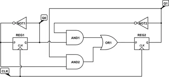
For a 2-bit counter, this looks like

schematic

simulate this circuit – Schematic created using CircuitLab

If you make a truth table, you'll see that the lsb (Q0) flips every clock, and the msb (Q1) becomes 1 for the codes 01 and 10. Check that this is a 2-bit binary counter. Extending the logic to 3 bits, with both Q0 and Q1 becoming 0 whenever Q2 becomes 1 is left as an exercise.

While we're at it, you should get in the habit of labeling your least significant bit 0 (as in Q0). In your proposed truth table you've got the order reversed. This habit will make life easier when you deal with arithmetic.

The synchronous approach is more complex than simply feeding the output of each FF to the clock of the next one (which will produce a binary counter). However, it is far more powerful and straightforward when making anything more complicated than a simple binary counter, and it gets around a major set of problems collectively called skew delay. Just take my word for it - by the end of your course you ought to be covering that, but don't worry about it for now.

WhatRoughBeast
  • 59,978
  • 2
  • 37
  • 97
  • thanks to all of you, and to @WhatRoughBEast -- I'd have voted for your answer too if i could. Looking at it now I think i get it, and i will take your suggestion. FYI this came up at the tail end of an electronics course, and in the course of three lectures we covered logic and gates and all that, but I'll be honest and say that if you asked me about any of it I am/was lost as all heck, and got to the point of "I give up just get me through the final." (There are classes I've had where I felt I got out of the class with a solid understanding of the material. QM was one. This was not). – Jesse Dec 16 '14 at 05:00
  • Jesse, just to let you know, this proposal is the same as my proposal. I just assumed that you would have learned state machines in the same course and that that terminology would have made you immediately recognize the structure. Great schematic, Beast! – PkP Dec 16 '14 at 21:01
-1

Well, D flipflip is one which will give out whatever input is fed in. Some thing like if you give a logic one as input when the clock is rising ( or the other way ) then it will store one and give out one till next transition.

Its Basically an SR flipflop. The data goes to S input and inverted data goes to R input