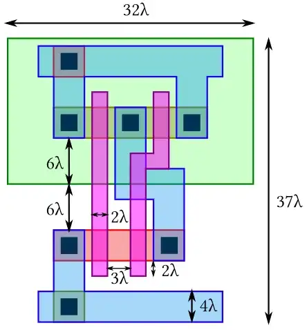
I always hear about process size improvements in the news, but could never figure out how it translates into dimensions of a logic gate. I found a chapter from Weste's CMOS VLSI Design, that contains figures which looks like things I create when playing KOHCTPYKTOP. There's a figure of a 3-input NAND gate, but none for a simple 2-input NAND. So I used Inkscape to draw my own, based on Mead & Conway's design rules mentioned in the chapter:
(I have no idea about the spacing around the well tap, I made it just 1 lambda)
So if I were to just plug in the current state of the art process size, which is supposedly 14 nm in 2014, can I say that the size of a NAND gate is about 448×518 nm²? Or is it possible to design it even smaller?