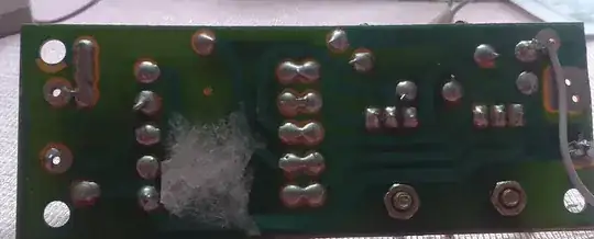
5

A friend brought this circuit to me and asked me to explain the working.

12v DC to AC circuit To viewenter image description hereenter image description here

I decoded the following schematic from the PCB.

schematic

simulate this circuit – Schematic created using CircuitLab

In the primary coil of the transformer I measured about 19KHz 14VAC. I am unable to understand how oscillation is being produced in the circuit. C1 and L1 looks like a tank circuit but I don't see how its oscillations are being fed to the PNP transistor and a specific feedback path.

Kindly help me decode the working of this circuit.

EDIT: It seems I mistaken the transformer primary winding taps to be short in my description. So the transistors are not short circuit or parallel.

vyi
  • 761
  • 10
  • 21
  • 1
    Your schematic is missing a transistor and a capacitor. I see 2 transistors and 3 capacitors on the PCB. – brhans Dec 08 '14 at 16:51
  • @brhans You are right. I've updated the description. Its interesting that the third capacitor is connected between the middle terminals of the two transistors BUT the middle terminals are short circuit as well( I checked with a continuity tester ). – vyi Dec 08 '14 at 16:56
  • I can see from the PCB that you are incorrect. The transistors are not in parallel. Only their emitters are connected together. Both bases and collectors appear to connect to different terminals on your transformer, and the transformer also appears to have many more connections than you show in the schematic. Without an accurate transcription of the circuit no-one could ever even begin to guess how its supposed to work. – brhans Dec 08 '14 at 17:06
  • @brhans You're right. I've corrected the schematic. The transformer circuit is a scarey one. – vyi Dec 08 '14 at 18:17
  • 1
    Btw. while googling for the used transistor datasheet I stumbled over this here http://www.circuitsdiy.com/cfl-emergency-kit-push-pull-application-12volt-18watt/ – PlasmaHH Dec 08 '14 at 23:38
  • This is the same circuit as i am using. Except that the transistors are npn as said by @OlinLathrop and there is a capacitor in the circuit secondary whereas in the shown webpage there's a diode. I have confusion regarding the type of transistor. In one datasheet with similar figures 1351 the type was pnp and i assumed it to be a pnp. Olin Lathrop also pointed out that it makes no sense to have a pnp, so i think it has to be NPN. I will again modify the schematic. – vyi Dec 09 '14 at 02:59
  • I'm awarding the bounty to user Kamil for he pointed out the real_identity of this circuit and relevant literature. I've accepted answer by @OlinLathrop as it explains finely(in a very lucid language) the working of this circuit. I'm thankful to both the users. – vyi Dec 23 '14 at 18:06

3 Answers3

3

Your schematic

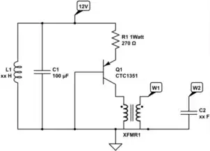
is incorrect. Check the connections again. It makes no sense to have a tank circuit directly across the power supply. It also makes no sense for the base to just be grounded.

For oscillation, there has to be positive feedback with a loop gain greater than 1 someplace at some frequency. Look particularly at the bottom connections of L1 and C1, and the base of the transistor. I'm sure your schematic isn't right in one or both of those areas.

Also look for a connection from the output side of the transformer back to the input side, particularly to the base or maybe the emitter of the transistor.

Update:

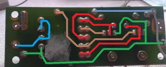
Your schematic is now:

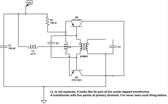
This still doesn't make sense. I am quite sure the bases of the transistors aren't driving the primary of the transformer. The connections as you show them would make a lot more sense if these were NPN transistors with the emitters grounded (where you show the collectors), the collectors driving the primary (where you show the bases), and the bases driven by the LL winding of the transformer. That might almost make sense, but it's hard to visualize with the broken schematic.

Update 2

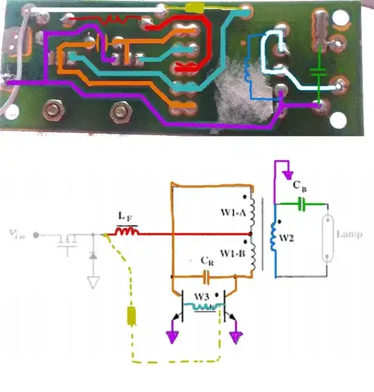
As I said last time, and you ignored in subsequent questions, I think you probably have something like this:

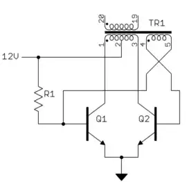
This is a classic push-pull configuration with low side drivers on each end of the primary and power applied to the center tap of the primary. The circuit arranges Q1 and Q2 to turn on alternately, which causes a net AC thru the primary.

The small feedback winding, arbitrarily between pins 4 and 5 in this example, is used to drive the bases of the transistors, and provides the feedback to make the whole thing oscillate. R1 provides the bootstrap current to get things going initially, and to supply some net bias current once things get going.

Consider everything off and the 12 V switched on. Both Q1 and Q2 start to conduct. However, there will be some inevitable imballance, so one of them will conduct a little more. Let's say Q1 is conducting a little more than Q2. That puts a net current thru the primary with the "dot" side being low voltage and the not-dot side high voltage. In the short term, the feedback winding will re-enforce this imballance. Note the orientation of the dots. The base of Q1 will be driven high relative to the base of Q2, so the feedback creates a sortof of "runaway" condition to amplify any imballance, which causes more imballance, which is amplified, etc.

However, the feedback is inherently AC coupled. Eventually the net current thru the primary reaches the maximum it can be, the current levels off, the magnetic field in the transformer therefore stops changing, and Q1 will stop being driven harder than Q2. As the magnetic field decreases, Q2 is actually driven harder than Q1. This actively drives the whole circuit to the opposite full-current point.

Some of the other parts I didn't put in this schematic help set the oscillation frequency to be a somewhat predictable value. This is most likely what the capacitor across the primary is doing, although at some cost in effeciency. Are you sure the capacitor isn't across the small feedback winding? Setting it up to be a little resonant makes some sense to get a predictable frequency, and to have that frequency be less depedent on load changes.

Due to the greater than unity positive feedback, but it being inherently limited to AC, the whole system will keep oscillating as long as sufficient power is provided. This oscillation causes large magnetic flux changes, which are picked up by the secondary (pins 19,20 in this example), to provide power to elsewhere. Since this is thru a transformer, there is considerable design range in the turns ratio from the secondary to the primary, and therefore in the output voltage relative to the input voltage. Both significantly higher and lower are possible.

Olin Lathrop
  • 310,974
  • 36
  • 428
  • 915
  • Ahh.. You're right. I've made mistake while decoding the circuit. I will update the schematic with the correct one. Thanks. – vyi Dec 08 '14 at 17:03
  • @vvy: Ping me when you have updated the schematic so that I can try to answer your question. – Olin Lathrop Dec 08 '14 at 17:09
  • I've updated the schematic and wow, Its entirely a different circuit. I realized that using continuity test on inductor terminals is a Gross Mistake.. – vyi Dec 08 '14 at 18:22
  • I've modified the circuit with npn transistors in the rational configuration. Can you explain the oscillation action? – vyi Dec 14 '14 at 21:01
  • @vvy: No, you still have the transistors hooked up strangely. Try the way I said. – Olin Lathrop Dec 14 '14 at 21:49
  • I've tried to show the pcb traces with colored line in the newly added image. I couldn't find any connectiom from the secondary of the transformer back to the base or emitter. I've not even found a legitimate datasheet source for the transistor type ctc1351. What should I do now? Also take a look at [this](http://www.circuitsdiy.com/cfl-emergency-kit-push-pull-application-12volt-18watt/) – vyi Dec 15 '14 at 17:50
  • Whoever downvoted this: It would be good to know exactly what you think is incorrect, misleading, of badly written. – Olin Lathrop Dec 22 '14 at 18:22
  • I didn't ignore your words, rather I couldn't understand/apply what you meant. Frankly speaking, I am an analog circuit phobic kind of guy. Please take no offense of my not being able to implement your suggestions. Your detailed answer gave me an insight of whats happening inside this circuit. Thanks a tons. – vyi Dec 23 '14 at 17:48
  • @vvy: If you don't understand a answer, ask about the specific parts you don't understand. Don't just continue on as if the answer was never given. – Olin Lathrop Dec 23 '14 at 18:20
  • I see your point. I did that out of my habit, I thought I shouldn't ask too many questions and do my homework well, but it seems I failed to understand the homework. I see that my behavior appeared ignorant, I'm really sorry about it. Next time I'd try to be more elaborate. Thanks. – vyi Dec 23 '14 at 18:27
3

I compared your PCB with Current-fed self-oscillating Royer inverter from document linked below. There are few differences:

  • additional resistor (I guess it helps with startup)
  • your inverter has no separation between primary and secondary (output ground is connected with input ground)
  • there is no transistor at input (to turn it on and off)
  • there is no diode at input (to protect power source from back-EMF from big coils)
  • there is no load on your PCB

Here is proof:

enter image description here

Here is explanation:

enter image description here

Sorry about that scan, but I see no point to rewrite it.

Here is source of schematic and scan:

The LCC Inverter as a Cold Cathode Fluorescent Lamp Driver by Joel A. Donahue, P.E. and Milan M. Jovanović from DELTA Power Electronics Lab., Inc.

link

Kamil
  • 5,926
  • 9
  • 43
  • 58
  • You decoded the circuit in a way better than I did. Thanks for putting in all that effort. Can you also tell me how you came across this literature? – vyi Dec 23 '14 at 17:58
  • Few years ago I was reading some magazine about electronics and there was article about very simple inverter for CCFL lamp. I didn't remembered Royer name, but I remembered that it was "self oscillating ccfl inverter". I googled that and found it. – Kamil Dec 23 '14 at 18:21
2

Your schematic is still messed up, this answer is based on low component count and how transistors are connected on PCB.

It looks like some CCFL driver with topology based on Royer oscillator.

From Wikipedia:

A Royer oscillator is an electronic oscillator circuit based on a relaxation oscillation, saturable-core transformer. It is used for DC to AC low frequency inverters. It was invented and patented in 1954 by George H. Royer. It has the advantages of simplicity, low component count, rectangle waveforms and easy transformer isolation.

And here is example of CCFL driver with current-fed self-oscilating Royer inverter topology:

enter image description here

Image source: link (Royer oscillator is on page 2)

Kamil
  • 5,926
  • 9
  • 43
  • 58
  • Good find or memory. The Royer outputs square waves. I was thinking based on the question that the circuit pictured in the question was a harmonic oscillator (sine wave output) but most likely it isn't. (continued in the next comment due to comment lenght limit!) – Fizz Dec 22 '14 at 03:37
  • There are several flavors of the Royer oscillator. The one with an inductor (LF) in series with the center tap (which you depict here, but which isn't in the one shown on Wikipedia) is called "current-fed Royer Oscillator" in some books such as Pressman et al., which has a detailed analysis of the MOSFET version of this circuit. The inductor LF limits current spikes; it's not otherwise needed to cause oscillation, i.e. it's not part of a tank. According to another book, Royer (with bipolar transistors) was a popular SMPS topology in the 1970s. – Fizz Dec 22 '14 at 03:39
  • Finally, my [now deleted] answer wasn't totally implausible. There are "Royer-like" sinusoidal output circuits which use push-pull topology! These don't have a Wikipedia page, but are discussed in an EDN letter exchange ["A Royer by any other name"](http://www.edn.com/Pdf/ViewPdf?contentItemId=4345505). – Fizz Dec 22 '14 at 04:52
  • 1
    If you put an appropriately sized capacitor (CR in the image above) in parallel with the center-tapped transformer primary, you get a "resonant Royer", which outputs sine waves because this capacitor and the transformer (center-tapped) primary form an LC tank! An EDN article by Jim Williams title "Tripping the light fantastic" goes into great detail in explaining the latter "resonant Royer", but the images for that article are currently broken on EDN; so, you are better off reading it from the EDN book *The Art and Science of Analog Circuit Design*. – Fizz Dec 22 '14 at 05:30
  • 1
    Also, I've changed the Wikipedia article so that it discusses both the square-wave- and sine-wave-output Royer; the article now contains a schematic for the latter as well. – Fizz Dec 22 '14 at 06:48