30

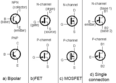
Transistor symbols are often drawn with arrows pointing in one direction or the other, depending on type, like in the following symbols:

Transistor symbols

But what is the arrow actually pointing at? And from where are they pointing? Is it the same principle behind it in each symbol and if so, why do they sometimes point FROM the transistor and sometimes TO it?

And why do the arrows point from different origins (sometimes base, emitter, gate, source etc) in different types?

Is there any general principle behind how the arrows are directed?

Tron
  • 347
  • 2
  • 4
  • 6
  • 3
    Looks like case D should be labelled "unijunction transistor". – John Honniball Dec 06 '14 at 08:55
  • That embedded image is gone because postimg.org is dead. – Navin Oct 09 '18 at 20:38
  • In Bipolar Junction Transistors the arrow is used to signify the BE junction. And the arrow's direction implies the doping characteristic of the base and the emitter, as the arrow is always drawn from the P-type material pointing to the N-type material. Always remember that the arrow head depicts the N-type and the arrow's tail depicts the P-type. – endrias Dec 25 '19 at 10:09

4 Answers4

14

For BJT's there is a PN junction between the base and emitter. The arrow indicates the order of the junction (base to emitter or emitter to base). An NPN has stacked N, P, and N doped channels. The PN junction (between base and emitter) goes from the center out. PNP likewise is the opposite.

Observations, not necessarily fact:

In a MOSFET, the body is often connected to the source. For an N-channel MOSFET, the source is N-doped and the body is P-doped, so the arrow points from the source to the body. Likewise, a P-channel MOSFET has the reverse condition. Interestingly, Wikipedia has symbols for "MOSFETS with no bulk/body" which have opposite arrow directions. I have no good explanation for why these are this way, though I suspect it might follow a similar pattern and the semiconductor topology is different from "traditional" MOSFET topologies.

Your symbols for b (FET) are JFET symbols. Here, the PN junction is between the gate and "body" (semiconductor section connecting the drain and source; I don't know what the correct for this part of a JFET is so I just called it the body because it takes the bulk volume of the JFET). For an N-channel, the gate is P-doped and the body is N-doped, so the arrow points from the gate in. The P-channel JFET is the opposite so the arrow points out of the gate.

I've never used unijunction transistors (case d), but looking at the wikipedia page shows a similar doping structure as the JFET, the only difference the lack of an insulated gate (names also have changed, apparently it follows the "BJT" type naming of base and emitter). I would not be surprised if the arrow direction convention follows the order of the PN junction (wasn't immediately obvious to me which type the example structure on Wikipedia was for).

Additional info:

Bipolar Junction Transistors

MOSFET

JFET

unijunction transistors
helloworld922
  • 16,600
  • 10
  • 54
  • 87
  • So to summarize the general principle, the arrow points from P-doped to N-doped area? That seems to make sense in most cases, except those "no bulk" symbols on Wikipedia that you mention where it's the other way around. If someone has an explanation for that, please add it. – Tron Dec 06 '14 at 11:48
  • Reading through the MOSFET wiki page: "If the bulk is not shown (as is often the case in IC design as they are generally common bulk) an inversion symbol is sometimes used to indicate PMOS, alternatively an arrow on the source may be used in the same way as for bipolar transistors (out for nMOS, in for pMOS)." It isn't clear to me why this is the convention. – helloworld922 Dec 06 '14 at 22:18
  • @helloworld922 I think the convention for MOSFETs having the same arrow directions as BJTs comes from similarities of an nMOSFET and a NPN BJT (arrow pointing out from the source/emitter) and a pMOSFET and a PNP BJT (arrow pointing into the source/emitter). I understand they're very different devices, but I think it's unnecessarily pedantic to not recognize the direct analog between nMOS/NPN and pMOS/PNP. – Shamtam May 31 '15 at 15:27
  • 1
    @helloworld922 "For an N-channel MOSFET, the source is N-doped and the body is P-doped, so the arrow points from the source to the body" I was under the impression that the arrow points from the body to the induced channel or alternatively "body to source"? This would also be consistent with the convention that arrows point from P to N. – cr1901 Apr 08 '17 at 07:03
  • @Shamtam crucially though, the arrow convention is the *opposite* of what you state, right? The arrow points out for a NPN and in for an nMOS. I think the analog you state is a great mental model, but the opposite arrow convention in the symbol creates lasting dissonance. – Heath Raftery Apr 04 '23 at 23:23
  • @HeathRaftery In the symbols in the OP, yes. I've commonly seen symbols for nMOS/pMOS where the body diode is omitted. These symbols look like the "FET" (really, a JFET) symbol in the OP, with an arrow on the S terminal pointing away from the transistor (nMOS), or with an arrow on the D terminal pointing towards the transistor (pMOS). This is what I was referring to in my comment, unfortunately not particularly clear. – Shamtam Apr 17 '23 at 03:11
  • Ah ha! That explains it then @Shamtam. The arrow *always* points to indicate the PN junction. In a JFET the gate is doped and forms one half of the junction. In a MOSFET it is not, so the substrate/body forms the junction instead. As I detailed over [here](https://electronics.stackexchange.com/a/661620/94854), the symbols turn out to be completely logical (which was a surprise to me, after 20 years of working with them). Now I see the same logic applies to JFETs, so I think that answer helps here too. – Heath Raftery Apr 17 '23 at 06:56
6

In short, the arrows show the current direction of a PN junction when forward biased.

  • In BJTs the PN junction is the base-emitter one.
  • In JFETs it is the one between gate and channel.
  • In MOSFETs it is the one which exists between the channel and the substrate (the terminal where the arrow is placed in the symbols you posted), which is not available externally. Note that when the substrate terminal is not shown in the symbol, the arrow is placed on the source and will point in the opposite direction, since the source has the same semiconductor polarity of the channel, which is always opposite to the substrate polarity: N-channel devices have P-type substrate and viceversa.
  • In UJTs (case d) it is the one between the emitter and the bulk semiconductor which connects the two base terminals.

Note that this convention is the same used for semiconductor diodes: the anode is connected to the part of the symbol which is a big arrowhead, and the anode is the terminal where the current enters the device when forward biased.

This doesn't mean that those junctions must be operated in forward bias conditions. This depends on the specific device type and operating conditions. E.g. JFETs are always operated with their gate junction reverse biased, whereas BJTs may work in different operating regions depending on whether their BE and BC junctions are forward or reverse biased.

4

The arrows in the bipolar transistors (emitter) show the direction of flow of conventional current. That is, current flow from positive to negative. Diode and LED symbols are the same.

EDIT: clarified, the emitter arrows.

John Honniball
  • 2,799
  • 11
  • 10
  • 1
    What about the mosfets? There is no current flow to the body terminal, is there? – John Dvorak Dec 06 '14 at 08:50
  • @JanDvorak No, you're right, I was thinking mainly of the bipolar transistors. But would a MOSFET conduct in that direction if it was biased appropriately? Isn't the body diode normally reverse-biased in operational circuits, so that it does not conduct? – John Honniball Dec 06 '14 at 08:53
  • This is not correct if you look at the symbols in the picture. In b) and c) the arrows point between gate and source, but no current flows between gate and source. – Tron Dec 06 '14 at 08:53
  • @Tron OK, I was thinking of the bipolar transistors. – John Honniball Dec 06 '14 at 08:54
  • re edit: but what about the other cases? ;-) – John Dvorak Dec 06 '14 at 08:59
  • 2
    @JanDvorak I have no idea; MOSFETs weren't invented when I started with electronics :) – John Honniball Dec 06 '14 at 09:01
2

About the bipolar transistor symbol.

First transistors were made with needles tucked into a germanium crystal, and were derived from point contact germanium diodes.

Galena diodes (for radio) used also nails set over the crystal surface, not soldered connections.

The symbol is litterally that. A specific junction transistor symbol once existed, but the point-contact symbol sticked.

TEMLIB
  • 3,347
  • 1
  • 14
  • 21