During my mosfet switching power dissipation I went through the Vgs curves of the MOSFET during its turn-ON state.Here i found that the Vgs curve remains flat during the miller plateau region. Why is it so? What exactly is happening to the Vgs growth here? Could somebody give clear cut explanation here?
Asked
Active
Viewed 1.0k times
3
-
Also relevant: http://electronics.stackexchange.com/questions/83712/gate-capacitance-and-miller-capacitance-on-the-mosfet , http://electronics.stackexchange.com/questions/74867/relationship-between-the-gate-charge-graph-and-the-vgs-waveform , http://electronics.stackexchange.com/questions/66660/why-is-the-gate-charge-curve-miller-plateau-of-mosfets-dependent-on-vds – gsills Dec 04 '14 at 05:11
3 Answers
9
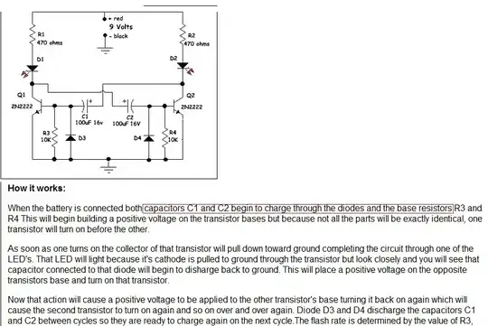
Here's a typical MOSFET switching circuit, with one component, normally hidden inside the MOSFET, here explicitly drawn on the circuit as C1.
There are actually capacitances between each pair of electrodes, but Cdg (=C1 here) is especially important in this configuration, so we can (to a first approximation) ignore the others (Cgs and Cds).
The reason for its importance comes from the relatively large change in Vds caused by a small change in Vgs, which causes a relatively large current through C1 opposing the current supplied by the driver. This has been known as the Miller effect, and Cdg as the Miller capacitance, since at least the early 1930s.
simulate this circuit – Schematic created using CircuitLab
So consider what happens when V1 switches from 0V to 5V.
The MOSFET is initially switched off, so Vds=100V. Vgs increases as the gate capacitances Cgs and Cdg charge in parallel through R1. You can estimate these capacitances from the slope at the start of the Vgs curve.
When Vgs passes the threshold voltage, M1 starts to turn on, and Vds starts to fall. Now there is a current through Miller capacitance C1 (Cdg), almost equal and opposite to that through R1, so Vgs remains flat (the plateau). I=C1* dVdg/dT
When the transistor is fully on (saturated), Vds=0 so this current ceases, and Vgs increases to 5V as Cgs and Cdg complete charging.
Much the same happens on switching off, so a good MOSFET driver must both source and sink current, probably better than the 100 ohm resistor R1 on the drawing.
Check the rise times on a datasheet's Vgs curves against the datasheet capacitance values and driver impedances, they should all make reasonable sense given the above explanation.
7
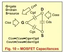
The MOSFET has two kinds of switching behavior: inductive and resistive. As you mentioned the "miller plateau", so i assume yours are an inductive switching. It is affected by the parasitic capacitances between the device’s three terminals, that is, gate-to-source (\$C_{gs}\$), gate-to-drain (\$C_{gd}\$) and drain-to-source (\$C_{ds}\$) capacitance as below.
Many docs and datasheet gives the "Vgs curves of the MOSFET during switching on" but don't give the circuits it is derived. I don't know your circuit, assume you have a similar circuit as below.
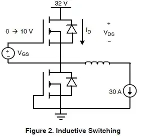
During turn on, capacitors \$C_{gd}\$ and \$C_{gs}\$ are charged through the gate.
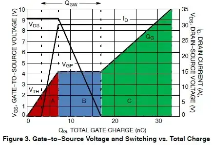
The relative regions in the above graph related with the familiar MOSFET working region as below:
As the OP concerns about why the Vgs curve remains flat during the miller plateau. At this region, the \$I_{D}\$ is limited by the external circuitry. From Figure 4, you see if \$I_{D}\$ is fixed, then \$V_{gs}\$ is fixed. At this time, \$C_{gd}\$ is charged. And the charging current is only limited by your series resistor on the gate. And is constant at this stage. As the voltage on \$V_{gd}\$ is increasing, the \$V_{ds} = V_{gs} - V_{gd}\$ decreasing.
For more details, you can refer to Ref 1.
Refs:
- “Power Electronics, converters, Applications and Design,” Mohan, Underland and Robbins.
diverger
- 5,828
- 5
- 43
- 79
-
I understand your explanation on what is happening to the current-voltage curves. But here i need an explanation as to what actually is happening physically inside the mosfet to keep that particular region flat? – IamDp Dec 04 '14 at 05:50
-
Bravo for relating Miller plateau to \$I_D\$ and the \$V_{GS}\$ vs \$I_D\$ characteristic curves. IMHO, any answer that omits these is defective. +1 – Math Keeps Me Busy Aug 27 '23 at 23:56
0
As Vgs increases past the threshold Vgsth Rds decreases allowing Id to flow. For resistive loads Vds also begins to drop. All of the current discharging Cds flows into the drain as does the load current and the current through Cgs. The gate current Ig derived from the source charges Cgs and discharges Cgd. Thus the rate of increase for Vgs is determined by the portion of gate current charging Cgs. As Vgs increases, Rds decreases (by channel enhancement) until all the available current flows into the drain. The current available to Cgd is the gate current. Since all Ig flows into the drain through Cgd none can flow into Cgs If Cgs cannot charge then Vgs is fixed at the Miller plateau. Vds=Vgd+Vgs. Therefore the drain voltage can change only as fast as the voltage across Cgd (Vgd) allows based on its current flow which is limited to Ig. As Vds decreases the load produces more current which reduces the current through Cgd. This allows a small increase in Vgs until all current flows into the drain. This continues until Vds is as small as it can be. A rise in Vgs may or may not be discernible on an oscilloscope. For inductive loads bypassed with a diode, the inductance acts like a current source for fast switching. When the transistor is off all the load current flows through the diode.As Vgs increases past the threshold Vgsth Rds decreases allowing Id to flow. This time a portion of the load current flows into the drain. The rest remains in the diode. As long as there is diode current Vds will remain at Vdd+Vdiode. Therefore the drain cannot demand current from Cgd or Cds. Thus Vgs keeps increasing until Rds is low enough to absorb all the load current (the diode current is zero). At this time the drain voltage begins to drop. The rest of the discussion is as before except there is no load current increase as the drain voltage decreases. Id is already at maximum. When the drain voltage stops changing, the current through Cgd will return to its appropriate portion and Vgs will rise to its design value based on Rdson. The Miller voltage should be higher with an inductive load. So to answer your question, During the Miller region
- Vgs is constant inductive load, rises a little, resistive load
- Channel enhancement is constant inductive load, more enhanced, resistive load
- Rds is constant inductive load, decreases a little, resistive load
- Id is constant inductive load, rises to load demand, resistive load
user128457
- 11
- 1
-
Please format your answers, maybe put a break in between for readability. Thanks – Voltage Spike Oct 31 '16 at 21:07