I took some pictures of a Microchip EPROM die from the late 80s / early 90s (I can't recall the exact part number). The wire bonding pads are surrounded by a comb-like structure. What is the purpose of this structure? 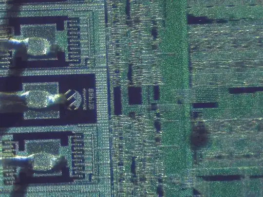

Asked
Active
Viewed 1,468 times
11
Scott Lawson
- 387
- 2
- 10
-
It would be interesting to see if the output pins and address pins look similar. The 24-pin EPROM pinout is pretty standard- the 12 address pins are grouped (with Vcc and Vpp in there) and the 8 output pins are grouped (with Vss in there). – Spehro Pefhany Nov 30 '14 at 23:21
3 Answers
11
At this writing, there are two "answers" that are total guesses - and wrong at that too.
These comb structures are as you might expect to see when you want to induce breakdown at a precise location and into controlled structures rather than else where in the chip. These are in the TOP metal layer, the combs are there to give lots of sharp edges to promote an excessively high ESD event to conduct at that location.
The diode and ESD clamping structures are by necessity in the Silicon.
These are very very far from being the transistor structures which are in the Si at least 3 - 7 metal layers down.
Look at lightning arrestors in the larger world. You will see these exact same things there.
Call it a belt and suspenders approach. Or rather a last chance, the actually ESD structures are rated for much lower voltage events.
placeholder
- 29,982
- 10
- 63
- 110
-
3-1 for failing to explain why the structures are connected to ground on one side and Vcc on the other. – Dave Tweed Dec 01 '14 at 02:51
-
1@DaveTweed guessing again I see. I didn't say they are connected to ground. There isn't enough information to warrant that assumption. What is that pin function? I don't know. – placeholder Dec 01 '14 at 02:56
-
-
From my POV, when I compare the answers I see one answer claiming that everyone else is wrong, and they are right, because of, well because they are, and another answer that at least tries to back this up with some external sources. – PlasmaHH Dec 01 '14 at 22:11
5
They are probably large p-MOS and n-MOS transistors that are used for ESD protection on the bonding pads. Here is a reference that shows various bonding pad designs in detail (in general this information is not easy to come by- IC manufacturers seem to treat ESD protection as a kind of trade secret). Image taken from the above pdf:

I don't recall Microchip ever making memory EPROMs. Is this part of an EPROM microcontroller?
Edit: Just looking at a Microchip PIC16C57, which is probably from a similar era. There are similar patterns on either side of most of the pins (which are I/O) but on only one side of the input-only pins such as T0CKI, /MCLR/Vpp, OSC1. So the structures appear to be drivers on one side and ESD protection circuitry of whatever kind on the other side.
Spehro Pefhany
- 376,485
- 21
- 320
- 842
-
Certainly the exact details of any specific IC fab process are considered trade secrets, at least until they become commonly known by multiple vendors. It's rare to even see die photos (top layer). – MarkU Nov 30 '14 at 21:52
-
I left the chip at home so at the moment I can't look up the exact part number. I think it was similar to the [27HC64](http://www.datasheets360.com/pdf/-7829273433840719317), which Microchip sold around 1990. I believe the chip I have has a few less pins though. – Scott Lawson Nov 30 '14 at 21:55
-
@ScottLawson Thanks! Obviously, from that datasheet, they did make EPROMs in that era. I was interested in confirming that it was a CMOS process, which it was. – Spehro Pefhany Nov 30 '14 at 22:02
-
It would be really interesting to see how you explain how these "MOSFET's" are made in ONLY Metal with no Silicon around. -1 for guessing. – placeholder Nov 30 '14 at 23:49
-
1@placeholder How do you know there is no silicon around- it is obviously on top of a silicon die so you're seeing something else. What would look different to you if those were transistors? – Spehro Pefhany Nov 30 '14 at 23:57
-
Well ask yourself, what is _ON TOP_ off a Silicon Die? the answer is Metal. You don't wire bond to Si you wire bond to the Metal _ABOVE_ it. You didn't know that? Further proof. How do I know that your answer is a guess? Because I design Si for a living, I consult on ESD structures in Silico and used to share a lab with the inventor of modern ESD protection. This answer is flat out wrong, rudimentary research would have told you that. – placeholder Dec 01 '14 at 02:53
-
Okay, it's wrong, fine. I think we all see the metal and we see the interdigitated pattern connected to the metal bonding pad. So what would the difference be if those were (say) N-channel transistors as in Fig. 17-13 in Hans Camenzind's book. How can I see the difference? – Spehro Pefhany Dec 01 '14 at 03:08
-
I'm not sure what you are asking. While the poly for the gates are interdigitated it would be rare (and silly) to also duplicate that structure in metal simply because you'd lose conductivity. It's better to have a strap of Metal with contacts (multiple) running down to each transistor finger. The photograph in your now added picture does NOT show the same thing as in the OP - That looks more like the a moat structure around each individual transistor, but one would have to know more about the process , # of metals etc. before making any conclusions. – placeholder Dec 01 '14 at 10:53
0
Those structures are the large transistors required to drive the pins that are used as outputs.
Dave Tweed
- 168,369
- 17
- 228
- 393