0

I have the following circuitry: enter image description here

PWM-2V8 is a square 50% 40kHz signal as this (R37 not populated on this capture): enter image description here

On P8, I get the following signal which is distorted and the duty is more like 65%: enter image description here

Q1 = Q2 = 568-8001-1-ND

Q3 = 568-6084-1-ND

I have tried R37=0 and R38=1k but it's still the same problem.

Can anyone explain to me what I don't get 50% at P8 and how I can fix it?

gregoiregentil
  • 651
  • 6
  • 19
  • 4
    Your schematic would be much easier to read if it were [conventionally drawn](http://electronics.stackexchange.com/questions/28251/rules-and-guidelines-for-drawing-good-schematics), with ground going down, and higher voltages at the top. Also, though you mention "mosfet" in the title, I don't see any MOSFET in your schematic. – Phil Frost Nov 27 '14 at 19:44
  • +1 to @PhilFrost's comment. That is a *horrible* drawing. – Connor Wolf Nov 27 '14 at 21:26

2 Answers2

3

It's called storage delay. Essentially, the base-emitter junction has some capacitance, and when you saturate the transistor, this capacitance is charged. To turn the transistor off, you must discharge this capacitance until you get down to the point where the transistor comes out of saturation, and starts to turn off.

Working against you is the Miller effect, which makes this capacitance look (from the perspective of the thing driving the base of a common-emitter BJT) much bigger than it is.

Some solutions you might consider:

  • saturate the transistor less
  • put a small capacitor in parallel with the base resistors
  • use MOSFETs (so you can eliminate base resistors, decreasing source impedance and thus discharging the capacitance faster)
  • avoid common-emitter topology
  • use a baker clamp
  • use a Schottky transistor (or make one with a discrete Schottky diode)
Phil Frost
  • 56,804
  • 17
  • 141
  • 262
1

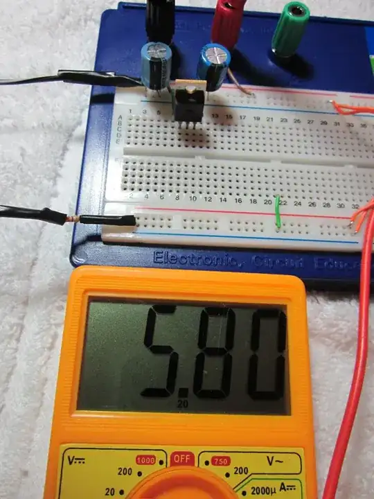
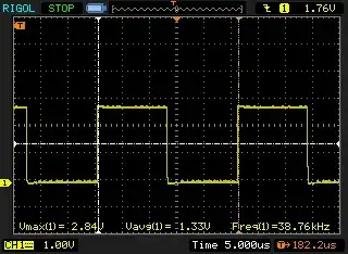
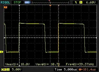
I don't think that the problem is related to the storage delay, because the working frequency is far too low (38 kHz according to capture) for this capacitance to show up.

Looking to the diagram one notices that the base current in Q3 is very big. When it is turned ON, the base voltage is at 19.3 V. The current from base node to ground (through Q1) is about 19/R43=19 mA. Most of those 19 mA comes from Q3 base. And for this transistor (ic max = 100 mA, hfe=100 minimum), you only need 1 mA in base current to reach saturation current.

I would not be surprised if Q3 has been damaged. Also Q1 might be damaged if you had tried it with R37=0 Ohms! Also Q2 should have a resistor of 47 kOhms between base and pin PWM-ZV8 negated. It is also very likely damaged.

Those three transistors should be replaced and new values for resistor calculated. For instance: R38=not populated, R37=47 kOhms, R43=18 kOhms, and a resistor of 47 kOhms for Q2.

Roger C.
  • 2,205
  • 1
  • 9
  • 12