I'm trying to make a NOT gate, but with a PNP transistor instead of NPN. What would a wire diagram look like for a NOT gate with a PNP transistor?
I'm trying to make a NOT gate, but with a PNP transistor instead of NPN. What would a wire diagram look like for a NOT gate with a PNP transistor?
It's the mirror image of the NPN solution: emitter to Vcc instead of ground, load resistor between collector and ground instead of between collector and Vcc.
edit
Like JustJeff says, make sure your input high voltage is high enough. If it is less than Vcc - 0.6V the transistor will be always on, or at least conduct partially, which shows when your LED isn't completely off. You can make the base voltage higher by adding a resistor from base to Vcc. Together with the base resistor it will form a divider. Example: say Vcc = 5V and your input high voltage is 4.2V. That's too low, the transistor will always be off. If you place a resistor between base and Vcc the same value as your input resistor, the base will be at 4.6V and the transistor will be off.
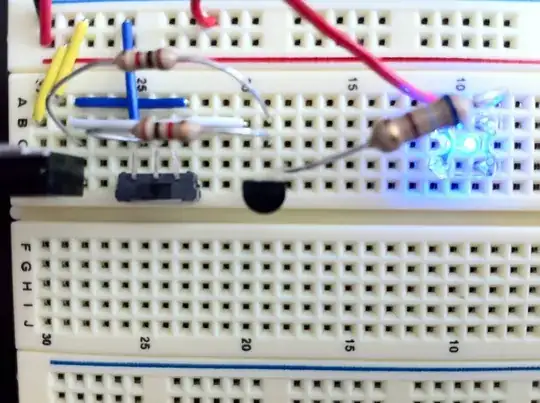
It seems that you want an inverter in the sense that you want to drive an LED on when you input a logic low, and off when you input a logic high. Something like this would do that:
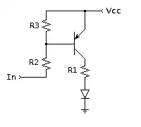
Values for the resistors depend on your supply voltage, and on what you're driving the input with. Assuming Vcc of 5V, R1 in the range of 470 ohm to 1K would be a fair choice, regardless of the input device. For a CMOS stage (or a switch between Vcc/Gnd) driving the input, R2 and R3 about equal and about 1K to 5K ought to do. For a TTL input, R2 should probably be about 3 or 4 times the value of R3, e.g., R3=680 ohm and R2=2.2K, because TTL doesn't guarantee anything more than 2.4V for a logic high, and you'll need to get the base to at least Vcc-0.7V, or higher, to shut the transistor off.