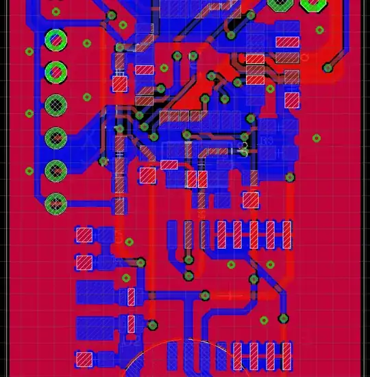
Below are two pictures of a portion of a PCB layout I did. The first shows the signal traces and the second shows the ground pour. U1 is an 8 MHz MCU, U3 an I2C sensor, U4 a RTC, and U2 a boosting power supply. The PCB is limited in size.
I don't have much experience in PCB layout, so there are probably a few fundamental flaws in the routing. It functions fine, though I can't comment on EMI. For VCC and GND I tried to use a gridded layout as much as possible, and add bypass caps as close as possible to the pins.
Now I'm trying to learn better PCB layout, e.g. signal return paths, reducing EMI, MCU having it's own little ground plane (Olin's answer), etc.
Can I achieve best practice layout on this fixed size PCB with 2 layers, or should I move to 4 layers?