7

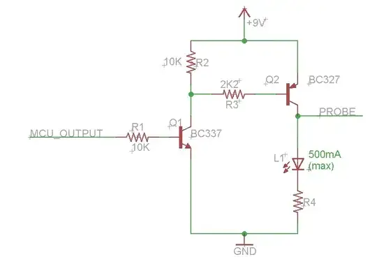
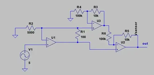
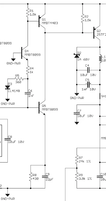
I have built a PCB with a set of high-side BJT drives shown in the schematic below. I'm using 8 of these to drive the columns of an 8x8 RBG LED matrix.

High-side BJT drive

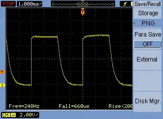
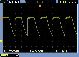
While debugging the board with my oscilloscope (with the load, i.e. L1 and R4, disconnected), I noticed that the circuit was showing a much longer fall time than I expected. I got 660us while I expected a fall time below 1us. Below are a series of scope shots I took.

Switching at 250Hz (T=4ms):

Scope shot at 250Hz

Switching at 1kHz (T=1ms):

Scope shot at 1kHz

Switching at 2kHz (T=500us):

Scope shot at 2kHz

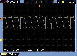
I'm switching the drive using an MCU through the MCU_OUTPUT signal and the scope shots were measured at the PROBE label.

The problem is that I need to switch the drive at around 14kHz, but above 1kHz, it doesn't even get to 0V during fall anymore. So above a certain frequency, the drive doesn't turn off.

Well, I only (sort of) understand how BJTs work in simple switch and amplifier configurations, so I'm puzzled with these results. I tried googling for it, but I don't even know what search terms to use. I'm stuck.

My questions are:

  1. Why is the fall time so much longer than the rise time on this circuit? The fall curve looks like that of a capacitor discharging, but I don't have a capacitor in the circuit. Or do I?

  2. How can I shorten the fall time on this circuit? Can I shorten it by changing the resistor values or the transistors?

I'm hoping I can learn something new about transistors with this opportunity.


Update: Testing with the load connected

I took Michael's answer into consideration and took another set of measurements with the load now connected. The scope shots are below. The results were much lower fall times, in the order of 660ns. That's 1000x lower than the original 660us I was getting with the load disconnected.

Switching at 2kHz with load connected (T=500us):

Scope shot with load switched at 2kHz

Switching at 14kHz with load connected:

Scope shot with load switched at around 14kHz

The end result is that the circuit I built is capable of switching my loads at the required frequency. It's just that I was making an incorrect measurement with the load disconnected.

Ricardo
  • 6,134
  • 19
  • 52
  • 85
  • Why is R1 so large? – Ignacio Vazquez-Abrams Oct 24 '14 at 02:58
  • @Ignacio - I calculated the values going from right to left. I figured that to get 500mA through R4, I'd needed about 3.5mA going through R3 (Ohm's Law and the 140x gain from the BC327-25). That, plus whatever comes through R2 is less than 5mA. I figured I could get that with 0.5mA going through R1, thus the 10K resistor. – Ricardo Oct 24 '14 at 11:22
  • 1
    Unrelated to your question, you may be interested in [this answer](http://electronics.stackexchange.com/a/55824/6494) about driving LEDs, specifically the "Linear Current Source" – sbell Oct 24 '14 at 12:49
  • @sbell - yes, I had seen the answer you linked, but it was long time ago. I'll take a fresh look at it again and see if I can take advantage of better methods for lighting my LEDs. Thanks for the pointer! – Ricardo Oct 24 '14 at 12:58

4 Answers4

13

Trying to evaluate your fall time with the load disconnected is not a useful measurement. As the PNP transistor turns OFF its collector terminal goes to a high impedance. That leaves the load to be the scope probe impedance which is likely to be 1Meg or 10Meg ohms. It is no wonder that it takes a long time for that size of load to discharge the small capacitance of the collector circuit and the scope probe capacitance.

Instead you should be looking at your switching time with the actual load hooked up. If the actual load is not available then at least add a test load resistor from the PNP collector to the GND rail. Size the resistor to dissipate power equivalent to the normal load that the circuit is meant to drive. Doing this you will see the real fall time and rise time of the circuit.

Update:

To get my point across take a look at the LT Spice circuit simulation below. I've drawn the circuit with a load consisting of a 10Meg ohm scope probe in parallel with 22pF of capacitance to simulate your actual scope probe capacitance plus some for the PNP collector terminal and the wiring. These pictures clearly show that the long fall time you are seeing is due to the fact that you have the load disconnected as I said above. It has next to nothing to do about the LED characteristics or the PNP saturation as another answer suggests.

enter image description here

enter image description here

Michael Karas
  • 56,889
  • 3
  • 70
  • 138
  • Well spotted, Michael!! I've just taken another set of measurements with the load now connected and you were absolutely right. The results were much lower fall times, in the order of 660ns. That's 1000x lower than the original 660us I was getting with the load disconnected. Thanks so much for clearing this up for me!! – Ricardo Oct 25 '14 at 19:44
  • I knew there was a capacitor hidden somewhere... – Ricardo Oct 25 '14 at 20:00
6

A possible reason could be that you are deep into saturation. The minority carries in the base have to be depleted before a depletion layer can form. The deeper into saturation you are, the more charge carriers you'll have in this junction and the longer it will take for them to leave.

Picture a bucket, and fill it with water. Make a hole in the bottom of the bucket. The more water you have, the longer it'll take for the water to get out.

There are three things you could possible do.

  1. Stop yourself from going into saturation so you are just at the border. Put a Schottky diode between base and collector, and it will clamp the the junction to prevent it from going into saturation.

Think of you filling the bucket enough to do the do the job. If you need a drink of water from the bucket, you dont need to fill the bucket up to the brim. So you fill the bucket with as much as water as you need. When it comes time to draining the bucket, you are now only draining what you need so the overall time will be faster since you arent draining the full bucket.

schematic

simulate this circuit – Schematic created using CircuitLab Couldnt find a Schottky so I just added a zener in there, for demonstration. But its supposed to be a Schottky.

  1. Add a series capacitor with the base. What this will do is apply a momentary reverse bias. Think of I = Cdv/dt, when you go from one discrete voltage to another, you'll get a +/- spike. That momentary pulse, will quickly push the transistor into cutoff because you're applied base voltage will be much higher/lower which will push the transistor harder.

Think of it as you tipping the bucket over for a very quick amount of time. You'll be dumping more water out than if you just let the hole you made do the job which in turns, speeds up the time you empty the bucket.

schematic

simulate this circuit

  1. Do both 1 and 2.
efox29
  • 11,827
  • 9
  • 56
  • 102
  • What do you mean by: "The minority carries in the base have to be released before the transistor will shut itself off.", Could you explain it a bit more? And how does the capacitor force them out? I am sorry if its offtopic or something, but I would really like to know. – Golaž Oct 24 '14 at 16:52
  • @Golaž added some additional stuff. Hopefully that helps. – efox29 Oct 24 '14 at 17:52
1

Looking at your circuit with everything in place, when Q2 switches OFF, its CE junction will go high Z, and the charge trapped in the LED will have no place to go except through your scope probe - 10 megohms? - to ground, which'll take a while.

If, instead of the voltage across the LED, you look at the current through it, you'll see that it quickly goes to zero when Q2 switches OFF, so the light from it won't tail off, it'll stop abruptly, which is probably what you want.

With that in mind, the voltage tail on turn-off is pretty much an artifact and won't affect how your circuit works unless, for some reason, you're using the voltage drop across the LED to effect some function.

The screenshot below shows the greatly reduced voltage decay on Q2 turn-off with 1000 ohms shunting the LED, because it allows the LEDs capacitance to discharge much more quickly than your scope probe will.

If you want to play with the (your) circuit, the LTspice circuit list is here, and if you don't have LTspice, it's available, free, here.

enter image description here

EM Fields
  • 17,377
  • 2
  • 19
  • 23
1

The first thing to do is to put R2 on the other side of R3. That alone won't make much difference in this case, but that way you have 10 kΩ trying to turn off the transistor instead of 12 kΩ.

The basic problem is that BJTs turn off slowly if the base is not actively driven to the emitter voltage. You have two BJTs in there, each taking a long time to turn off.

The solution for Q1 is easy. Don't run it as a grounded emitter amplifier, but rather a controlled current sink. Put R1 on the emitter instead of the base, and drive the base directly from the microcontroller pin. When the digital signal goes low, it will actively drive the base low and turn off the transistor quickly. When it goes high, the collector will act like a fixed current sink. This not only uses the transistor a bit more efficiently, but it guarantees it never saturates.

However, before we get into the details around Q1 we have to start with what Q2 needs. You didn't provide links to the transistor datasheets, so I'll just make up some number to use as example. You will have to use the correct numbers and redo the calculation accordingly. It looks like Q2 needs to handle some power, so let's say it can be counted on to have a gain of 25. Q1 can be small signal, so let's say it has a minimum gain of 50.

Q2 needs to supply 500 mA, so it's base current needs to be at least 20 mA. We'll put a resistor accross its B-E that draws 2 mA to turn it off fairly fast when the base current is removed. That means Q1 has to sink 22 mA minimum, so let's target 25 mA to leave a little margin. If the B-E drop of Q2 is 700 mV, then a 350 Ω resistor draws the 2 mA when on. We'll use the standard value of 360 Ω. Close enough.

Now we need to arrange for Q1 to sink 25 mA when the digital output is high. Again let's use 700 mV as the B-E drop. If the digital output is 3.3 V when high, then that leaves the emitter at 2.6 V. (2.6 V)/(25 mA) = 104 Ω, so we'll use the standard value of 100 Ω.

We can speed up Q1 a little quite easily by putting a cap across the emitter resistor. This will provide a small surge of current when first turning on, and will turn the it off more rapidly when the base is brought to ground suddenly by the digital output. Aiming for a 1 µs time constant puts the capacitor at 10 nF.

So here is the result:

This is probably good enough on its own, considering you are only switching at 14 kHz and only 500 mA. Regardless of the gain of your transistors, R2 will still drain the base of Q2 at 2 mA when Q1 is switched off. Any normal small signal transistor will be good enough for Q1. You need to adjust R1 so that Q1 sinks enough current to guarantee Q2 is fully on with the maximum load of 500 mA.

You can take this concept further, although I don't think it's necessary in this case. Here is a snippet from a buck switcher I recently used in a product:

Q5 is the switched current source. In this case its base is a 0-5 V digital signal out of a microcontroller (PIC 10F204). R8 sets the current W5 sinks when on, C9 is the speedup cap, and Q2 is the high side switch being controlled. The wrinkle in this case is that the falling edge of the digital signal causes Q1 to be turned on for a short time, but long enough to drive Q2 off quickly. R2 then holds Q2 off until Q5 is turned on again when the digital signal on its base goes high.

I have to go now. Take a look at the circuitry around Q4 and Q1 and see if you can figure out how they turn off Q2 quickly for a short time when the digital signal goes low.

Olin Lathrop
  • 310,974
  • 36
  • 428
  • 915
  • First of all, I'd like to thank you so very much for your fantastic answer. I really appreciate the time you spent looking at my circuit. But I have to ask, did you take into account the fact that I took the shots with the load disconnected? Michael Karas seems to think that the long fall times I was getting were artifacts of my measuring setup, that Q2 was being discharged through my scope probes resistance and capacitance. I ran a few more measurements and that seems to be the case. If you feel like sparing yet a bit more time on this, I would be really interested in your thoughts on this. – Ricardo Oct 25 '14 at 19:59
  • @Ricardo: Yes, the fall times will be much larger without a load. If the load is always there, then both the risising and falling edges need to be looked at with the load connected. In that case, what the falling edge does with no load is no indication of anything useful. But, what is the point of your question if you weren't experiencing problems caused by slow falling edges? I assumed that was the case else you wouldn't be here asking how to fix it. – Olin Lathrop Oct 26 '14 at 15:09
  • @OlinLathrop I'll try to take a stab at what Q1 and Q4 are doing in the circuit. First, Q1 appears to form a push-pull type arrangement with Q5. Note: a current through R1, downward, will cause Q1 to turn on. Q5 turns on/off the switching BJT (Q2) via the uC. When the uC pin is high, Q5 to turn on which turns on Q2. When the uC pin is low, we want Q2 to turn off quickly. Ideally, we'd like to pull Q2's base high to the positive rail to turn Q2 off quickly. Q1 is there to short out R2 and pull Q2's base to the rail when Q1 turns on. – mrbean Feb 20 '21 at 18:53
  • A rising 3.3V on the uC, causes a dV/dt appears across the capacitor that sends current upward. Q4 is normally off, so current travels through R5 and D3. A falling 0.0V, causes a dV/dt across the capacitor that sends current downward. This downward current causes Q4 to turn on. This is where things get a tad fuzzy. The downward current should case a voltage across R4 which drops the voltage on Q4's emitter below ground, which turns on Q4. How much I'm not sure. Note: series D3 and R5 is in parallel with series Q4's B-E/R4. Does D3 have a parasitic capacitance that comes into play a well? – mrbean Feb 20 '21 at 18:54
  • Either way, Q4 turns on which causes a current to flow through R1. The current hopefully causes an IR drop high enough across R1 (~0.7V) that Q1's B-E junction turns on briefly. Note: The details around D3/R4/Q4/R4 are a little fuzzy. Hopefully this is roughly the idea. – mrbean Feb 20 '21 at 19:01
  • Another question I have is how to calculate the values for capacitor (C6) and resistor (R4) to achieve 0.7V across Q4's B-E junction when the uC pin goes low. – mrbean Feb 20 '21 at 20:29
  • Nevermind, I think I get it. When the uC pin is at 3.3VDC the capacitor charges up to 3.3VDC. After enough time the capacitor is fully charged and looks like an open circuit. When the uC pin goes low, there is still 3.3VDC across the capacitor because voltage across a capacitor cannot change instantaneously. The capacitor, which looks like a voltage source (+ lead is now switched to ground) and places +3.3VDC across Q4 B-E and R4. The 3.3VDC across the capacitor, turns on Q4 which turns on Q1. – mrbean Feb 20 '21 at 22:13