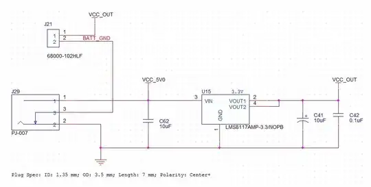
I am currently working on a similar problem. Got a handheld device and it should switch to battery supply and back based on an external voltage.
I came up with a pretty basic and draft design, here's the schematic:
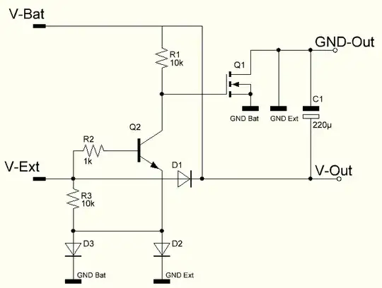
So what does it do?
This circuit basically switches the GND path of the battery on and off on your load, based on the state of V-Ext.
Case 1:
-> V-Bat connected, V-Ext disconnected
R3 pulls V-Ext to GND-Bat. Therefor Q2 is switched off and the gate of Q1 loads a charge via R1.
Q1 switches on, and GND-Bat is connected to the actual circuit.
Case 2:
-> V-Ext gets connected
Now, that V-Ext is connected, voltage on the base of Q2 increases, switching Q2 on. Therefor Q2 pulls the gate of Q1 to GND-Bat, discharging it and turning it off.
The battery is now disconnected. But keep in mind that a small current still flows through R1. About 1mA on a 9V battery.
D2 & D3 separate GND-Ext and GND-Bat. This is important! Both ground paths are needed for Q2 to switch properly, but they have to remain separated, otherwise you wouldn't be able to switch one at the output.
Case 3:
-> V-Ext gets disconnected, again
It's the same as Case 1, actually, with one little difference.
R3 pulls V-Ext to GND-Bat, and Q2 switches off, as before. However, it takes a while for the gate capacitance of Q1 to load properly. Meaning there's a delay in switching where no ground is connected and no closed circuit exists. Now, that's what C1 is for. It prevents a short voltage drop which could cause problems and flattens any ripple caused by connecting or disconnecting an external power source.
But how to calculate that delay? Easy! Look in the datasheet of the Mosfet you desire and look for the gate capacitance.
t_delay = 5 * R1 * Cgate
So if the gate capacitance is, for example 100pF, it'd be
tDelay = 5 * 10kOhm * 100pF
tDelay = 5 * 10,000Ohm * 0.0000000001F
tDelay = 0.000005s
tDelay = 5us
this formula calculates the time until the gate is fully charged, however, Q1 usually switches on, earlier. I like to overshoot a little with these thresholds.
I think C1 is way to large in this setup, btw.
Some final words:
This circuit is nothing else but a simple NOT gate (which would be Q2) driving the gate of Q1.
As mentioned earlier, this circuit draws a "standby current" from the battery as long as you also connect it to an external power source. You can decrease that current by increasing R1. However, since R1 is a factor in the formula for switching delays it will also increase your switching delay. I think it should be safe to replace R1 with 1 megaohm, though.
Also be careful with V-Ext. It is the primary input, meaning, this circuit will switch to V-Ext, even when it's way to small. Even if it's just 1V! Do not buffer V-Ext with a capacitor, it will ruin this setup. To prevent this you could use a voltage divider on the base of Q2. R3 also prevents V-Ext and therefor the base of Q2 from floating. Induced voltages of disconnected leads acting like an antenna are not a problem.
There were some messes in my previous post, I hope I fixed everything!