3

I'm trying to understand the standard TTL NAND Gate in TTL level. But confused with the transistor Q1 operation in the diagram below:

Two input TTL NAND Gate

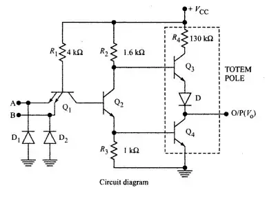
Apparently when A and B are together HIGH, the Q1 base-emitter junction is reverse biased. Collector-base junction is on the other hand forward biased. So the current flows through R1 and turns on the transistor Q2. So far so good up to here.

Here is my question: How can a BJT(probably npn) transistor such as Q1 can operate in such way? I mean when I learn about transistors the base emitter collector connections are very important. But from this Q1 I conclude that one can use base and collector interchangeably. Is that right?

user16307
  • 11,802
  • 51
  • 173
  • 312
  • A BJT is simultaneously both a transistor and a pair of diodes. – Ignacio Vazquez-Abrams Oct 23 '14 at 00:47
  • I dont understand how current flows this way in Q1. Could you expund on how the q1 operates in my diagram? – user16307 Oct 23 '14 at 00:50
  • 1
    Current cannot flow from the base to the emitter, so it flows from the base to the collector instead. – Ignacio Vazquez-Abrams Oct 23 '14 at 00:54
  • i think im confused because normally the base is a very small voltage just to trigger the transistor and the real current flows from collector to emitter. but in this case i noticed the base is directly connected to the Vcc. as you put it it acts like diode here. – user16307 Oct 23 '14 at 00:58
  • Yes, and that is the transistor model. But the diode model also exists simultaneously. – Ignacio Vazquez-Abrams Oct 23 '14 at 01:12
  • 1
    Theoretically bipolar transistors are only 2 opposed PN junctions, which would normally mean they can be used interchangeably - however usually the collector is made wider than the emitter [in turn wider than base] which makes the transistor asymmetric. As for the base and collector, they definitely don't have the same working and can't be switched around in terms of biasing. The configuration (common base, emitter, collector) can change though. – Mister Mystère Oct 23 '14 at 01:35
  • I also read that from Millman's microelectronics 2e, pp. 246 book that if at least one emitter input is LOW, then collector-base junction will be reverse biased. How can it be ? – curious_mind Mar 31 '23 at 05:30
  • I am beginner in electronics, but I struggle to understand if both emitter inputs are HIGH, can someone explain why exactly both junctions of Q1 will be forward biased ? – curious_mind Mar 31 '23 at 05:37

1 Answers1

3

As I'm sure you've learned, a BJT is composed of two back-to-back P-N junctions. Knowing this, allow me to redraw Q1 for you, using the diode model of a BJT:

schematic

simulate this circuit – Schematic created using CircuitLab

When the voltage on either of the emitters is below the threshold set by Q2 and Q4, the appropriate emitter diode is forward biased and current flows through it. When both emitters are above the threshold, current flows out of the collector instead, activating Q2 and in turn deactivating Q3 and activating Q4, pulling the output low.

Ignacio Vazquez-Abrams
  • 48,282
  • 4
  • 73
  • 102
  • 1
    R1 and Q1 are acting as a current source. If A or B (or both) are low, they take enough current away (current "sink") to stop Q2 conducting. However, when both are high, the current has no path left other than the forward biased base-collector, causing Q2 to conduct. – Alan Campbell Oct 23 '14 at 02:32
  • @Alan Campbell thanks i have 3 confusions here.. 1)why do you call it current source? 2)if R3 wouldnt exit Q2's emitter would be grounded, what woıld happen in that case? would current divides and equally flow through collector and emitter of Q1? 3) what should be the proper amount of voltage applied to A and B to reverse bias the emitter base junction? – user16307 Oct 23 '14 at 10:13
  • @user16307 Q2 base is 1.2V, so Q1 base is about 1.8V. Vcc=5V (TTL) I = 3.2/4K = about 0.9mA always flowing thru R1. 2) If you short R3, there is no current limit for Q2. It saturates, collector approaches 0.2V, Q3 and Q4 are driven to cutoff. 3) If Q1 base is 1.8V then A or B need to be below 1.2V to come "on" and draw current from R1. – Alan Campbell Oct 23 '14 at 10:51
  • im still confused 1)why do you say " Q2 base is 1.2V, Q1 base is about 1.8V"? how do we know that? 2)i thought in TTL logic outputs and inputs are between 0 to 5V. in this case you tell that 5V is the Vcc. so what will be the output ON voltage (at Q4 collector)? – user16307 Oct 23 '14 at 11:47
  • Just to ask it here and not convolute the other thread more than it already is, If Q3 is off, how can Q4 be active and conduct without a path to do so? – sherrellbc Mar 17 '15 at 19:11
  • Q3 can only be off if Q2 is on and hence sinking the current from R2. This turns Q4 on. – Ignacio Vazquez-Abrams Mar 17 '15 at 19:17
  • @sherrellbc: I think I finally got your question. And it only took two months :P The conduction path for Q4 when Q3 is off is from the outside circuit, i.e. the next logic stage. – Ignacio Vazquez-Abrams May 19 '15 at 14:57