9

This question is about implementing a IIR filter in a FPGA with DSP slices, with very specific criteria.

Lets say you're making a filter with no forward taps and only 1 reverse tap, with this equation:

$$y[n] = y[n-1] \cdot b1 + x[n]$$

(see image)

Take the DSP48A1 slice from Xilinx as an example - most hard IP DSP slices are similar.

Lets say you have analog data incoming at 1 sample per clock. I would like to design an IIR filter that runs synchronously at the sample clock.

The problem is that in order to run the DSP slice at the maximum rate, you can't multiply AND add on the same cycle. You have to have a pipeline register between these components.

So, if you have 1 new sample every clock, you will need to produce 1 output per clock. However, you need the previous output 2 clocks before you can produce a new one in this design.

The obvious solution is to either process the data at double clock rate, or to disable the pipeline register so that you can multiply and add in the same cycle.

Unfortunately, if say you're sampling at the max clock rate of the fully pipelined DSP slice, neither of those solutions are possible. Is there any other way to build this?

(Bonus points if you can design a IIR filter that operates at half of the sample rate, using any number of DSP slices)

The goal would be to run a compensation filter for a 1 GSPS ADC in a Xilinx Artix FPGA. Their DSP slices can run just over 500 MHz when fully pipelined. If there is a solution for 1 sample per clock, I would like to try and scale the solution for 2 samples per clock. This is all very easy with an FIR filter.

single feedback IIR filter example

Ricardo
  • 6,134
  • 19
  • 52
  • 85
Marcus10110
  • 589
  • 3
  • 13
  • 1
    Just to clarify, there's no reason why you wouldn't have one output per clock cycle with the pipeline method, right? You're trying to minimize the latency down to one clock cycle instead of two, right? Depending on your situation, if you're using an integer for b1, then you could convert the multiply into a giant add including x[n]. – horta Oct 12 '14 at 01:48
  • right - since there is one input per clock, there needs to be one output per clock. latency isn't an issue either. the DSP slice only has a 2 input adder, and the taps are usually pretty big numbers, so you couldn't add b1 times in 1 clock cycle. the main limit is that the output needs to feed back in 1 clock, but it takes 2 clocks to produce. – Marcus10110 Oct 12 '14 at 04:19
  • 1
    I think you're still misunderstanding how a pipeline works. A pipeline potentially increases latency, but allows you to get 1 output for each input at each clock cycle. It's just that the result is now 2 clocks after rather than the ideal 1 clock after. The input would be the sequence like this: x[0],x[1],x[2],x[3],x[4] while the output would be at that same time interval y[-2],y[-1],y[0],y[1],y[2]. You're not losing any samples. Also, you're on an FPGA, so if you want to get more work done than what the DSP pipelines are designed for, utilize the fpga to parallelize the workload. – horta Oct 12 '14 at 06:44
  • That DSP is capable of doing a fused multiply accumulate in a cycle. It's unclear to me though if the output of a DSP slice can be connected to its own input with feedback in a single cycle. – jbarlow Oct 12 '14 at 08:24
  • horta - you're right about pipelining in general, but the problem is that the tab b1 in this case has feedback - meaning that a stage in the pipeline depends on the output of the previous value. if it always takes 2 clocks to produce the next output from the previous output, there is no way to produce 1 output per clock, regardless of how much latency you've added. jbarlow - you're right, the DSP slice has a 1 cycle fused option. However it can't run fast enough in this case. by adding the M register (see datasheet) you can reach 500 MHz.However then you can't multiply and add in the same clk. – Marcus10110 Oct 12 '14 at 18:14
  • Ah, I see what you're saying now Marcus. I'm thinking the only solution now is for you to create your own logic in the fpga part of it that allows you to perform a multiply-add in a single clock cycle while feeding output directly back to the input of this logic block. – horta Oct 12 '14 at 23:23
  • My usual answer to questions like this at work is "You have a very set implementation in mind... tell me the actual spec for the processing you are trying to do, lets see if we can do it another way" – Martin Thompson Oct 13 '14 at 13:18
  • you're right, and I'm already working on other options that are significantly different. the goal is to build a 1 GSPS oscilloscope out of a Artix-7 FPGA. The IIR filter is mainly for compensating the pass band, in case it's not flat. However since the scope will operate on short capture buffers, it's not a problem to filter the data after the fact at a lower speed - no need to stream continuously. doing the compensation filtering up front is just one idea that leaves more options open. This is also a good performance exercise to see exactly how fast and IIR can run, so I'm glad I asked. – Marcus10110 Oct 13 '14 at 18:35

2 Answers2

3

I haven't worked with IIR filters yet, but if you only need to calculate the given equation

y[n] = y[n-1]*b1 + x[n]

once per CPU cycle, you can use pipelining.

In one cycle you do the multiplication and in one cycle you need to do the summation for each input sample. That means your FPGA must be able to do the multiplication in one cycle when clocked at the given sample rate! Then you'll only need to do the multiplication of the current sample AND the summation of the last sample's multiplication result in parallel. This will causes a constant processing lag of 2 cycles.

Ok, let's have a look at the formula and design a pipeline:

y[n] = y[n-1]*b1 + x[n]

Your pipeline code could look like this:

output <= last_output_times_b1 + last_input
last_output_times_b1 <= output * b1;
last_input <= input

Note that all three commands need to be executed in parallel and that "output" in the second line therefore uses the output from the last clock cycle!

I didn't work much with Verilog, so this code's syntax is most possibly wrong (e.g. missing bit-width of input/output signals; execution syntax for multiplication). However you should get the idea:

module IIRFilter( clk, reset, x, b, y );
  input clk, reset, x, b;
  output y;

  reg y, t, t2;
  wire clk, reset, x, b;

  always @ (posedge clk or posedge reset)
  if (reset) begin
    y <= 0;
    t <= 0;
    t2 <= 0;
  end else begin
    y <= t + t2;
    t <= mult(y, b);
    t2 <= x
  end

endmodule

PS: Maybe some experienced Verilog programmer could edit this code and remove this comment and the comment above the code afterwards. Thanks!

PPS: In case your factor "b1" is a fixed constant, you might be able to optimize the design by implementing a special multiplier that only takes one scalar input and calculates "times b1" only.

Response to: "Unfortunately, this is actually equivalent to y[n] = y[n-2] * b1 + x[n]. This is because of the extra pipeline stage." as comment to old version of answer

Yes, that was actually right for the following old (INCORRECT!!!) version:

  always @ (posedge clk or posedge reset)
  if (reset) begin
    t <= 0;
  end else begin
    y <= t + x;
    t <= mult(y, b);
  end

I hopefully corrected this bug now by delaying the input values, too in a second register:

  always @ (posedge clk or posedge reset)
  if (reset) begin
    y <= 0;
    t <= 0;
    t2 <= 0;
  end else begin
    y <= t + t2;
    t <= mult(y, b);
    t2 <= x
  end

To make sure it works correctly this time let's look what happens at the first few cycles. Note that the first 2 cycles produce more or less (defined) garbage, as no previous output values (e.g. y[-1] == ??) are available. The register y is initialized with 0, which is equivalent to assuming y[-1] == 0.

First Cycle (n=0):

BEFORE: INPUT (x=x[0], b); REGISTERS (t=0, t2=0, y=0)

y <= t + t2;      == 0
t <= mult(y, b);  == y[-1] * b  = 0
t2 <= x           == x[0]

AFTERWARDS: REGISTERS (t=0, t2=x[0], y=0), OUTPUT: y[0]=0

Second Cycle (n=1):

BEFORE: INPUT (x=x[1], b); REGISTERS (t=0, t2=x[0], y=y[0])

y <= t + t2;      ==     0  +  x[0]
t <= mult(y, b);  ==  y[0]  *  b
t2 <= x           ==  x[1]

AFTERWARDS: REGISTERS (t=y[0]*b, t2=x[1], y=x[0]), OUTPUT: y[1]=x[0]

Third Cycle (n=2):

BEFORE: INPUT (x=x[2], b); REGISTERS (t=y[0]*b, t2=x[1], y=y[1])

y <= t + t2;      ==  y[0]*b +  x[1]
t <= mult(y, b);  ==  y[1]   *  b
t2 <= x           ==  x[2]

AFTERWARDS: REGISTERS (t=y[1]*b, t2=x[2], y=y[0]*b+x[1]), OUTPUT: y[2]=y[0]*b+x[1]

Fourth Cycle (n=3):

BEFORE: INPUT (x=x[3], b); REGISTERS (t=y[1]*b, t2=x[2], y=y[2])

y <= t + t2;      ==  y[1]*b +  x[2]
t <= mult(y, b);  ==  y[2]   *  b
t2 <= x           ==  x[3]

AFTERWARDS: REGISTERS (t=y[2]*b, t2=x[3], y=y[1]*b+x[2]), OUTPUT: y[3]=y[1]*b+x[2]

We can see, that beginning with cylce n=2 we get the following output:

y[2]=y[0]*b+x[1]
y[3]=y[1]*b+x[2]

which is equivalent to

y[n]=y[n-2]*b + x[n-1]
y[n]=y[n-1-l]*b1 + x[n-l],  where l = 1
y[n+l]=y[n-1]*b1 + x[n],  where l = 1

As mentioned above we introduce an additional lag of l=1 cycles. That means that your output y[n] is delayed by lag l=1. That means the output data is equivalent but is delayed by one "index". To be more clear: The output data delayed be 2 cycles, as one (normal) clock cycle is needed and 1 additional (lag l=1) clock cycle is added for the intermediate stage.

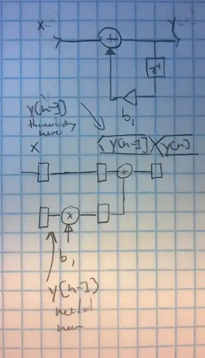
Here is a sketch to graphically depict how the data flows:

sketch of data flow

PS: Thank you for having a close look at my code. So I learned something, too! ;-) Let me know if this version is correct or if you see any more issues.

SDwarfs
  • 680
  • 3
  • 15
  • Nice Work! Unfortunately, y[n] = y[n-2] * b + x[n-1] isn't actually functionally equivalent to y[n] = y[n-1] * b + x[n] with latency. The form of a IIR transfer function actually looks like this: y[n] = x[n] * b0 + x[n-1] * b1 - y[n-1] * a1 - y[n-2] * a2 and so on. Your form sets b0 and a1 to 0, and instead uses b1 and a2. However, that transform actually produces a very different filter. If there was a way to compute a filter with the first denominator (a1) set to zero though, both of your solutions would work perfectly. – Marcus10110 Oct 30 '14 at 10:41
  • Well, you need to understand the "introduced lag" issue correctly. As example, a "data stream processing" filter should just forward its input as y[n] = x[n] would work correctly if it produces y[n] = x[n-1] as output. The output is just delayed by 1 cycle (e.g. the output index is offset by a fixed value relative to all the input indices)! In our example this means your function is `y[n+l] = y[n-1] * b + x[n]` with a fixed value for the lag `l` which can be rewritten to `y[n] = y[n-1-l] * b + x[n-l]` and for l=1 this is `y[n] = y[n-2] * b + x[n-1]`. – SDwarfs Oct 30 '14 at 13:07
  • For your more complex IIR filter you would need to do the same: `y[n+l] = x[n] * b0 + x[n-1] * b1 - y[n-1] * a1 - y[n-2] * a2` => `y[n] = x[n-l]*b0 + x[n-1-l] * b1 - y[n-1-l] * a1 - y[n-2-l]*a2`. Assuming you can do all the three multiplications in parallel (1. stage / 1 cycle) and need to do the to add the products together you need 2 cycles (1 cycle: add/sub first two product results, 1 cycle: add/sub the result of those two add/subs), you'll need 2 additional cycles. So l=(3-1)=2 giving you `y[n]=x[n-2]*b0+x[n-1-2]*b1-y[n-1-2]*a1-y[n-2-2]*a2`=> `y[n]=x[n-2]*b0+x[n-3]*b1-y[n-3]*a1-y[n-4]*a2` – SDwarfs Oct 30 '14 at 13:20
  • Of course for this to work your FPGA must be able to do in parallel: 4 multiplications and 3 additions/subtractions. Meaning you need resources for 4 multipliers and 3 adders. – SDwarfs Oct 30 '14 at 13:32
0

Yes you can clock at the sample frequency.

A solution to this issue is to manipulate the original expression so that pipeline registers can be inserted, while maintaining the desired output sequence.

Given: y[n] = y[n-1]*b1 +x[n];

this can be manipulated into: y[n] = y[n-2]*b1*b1 +x[n-1]*b1 +x[n].

To verify this is the same sequence consider what happens to the first several samples x[0], x[1], x[2] etc, where previous to x[0] all x,y samples were zero.

For the original expression the sequence is:

y = x[0],

x[1] +x[0]*b1,

x[2] +x[1]*b1 +x[0]*b1*b1,

x[3] +x[2]*b1 +x[1]*b1*b1 +x[0]*b1*b1*b1, ...

It is clear that it is necessary that b1 < 1, otherwise this will grow without bound.

Now consider the manipulated expression:

y = x[0],

x[0]*b1 +x[1],

x[0]*b1*b1 +x[1]*b1 +x[2],

x[0]*b1*b1*b1 +x[1]*b1*b1 +x[2]*b1 +x[3], ...

This is the same sequence.

A hardware solution in Xilinx library primitives would need two DSP48E in cascade. Refer to figure 1-1 in UG193 v3.6 for the port and register names below. The first primitive is multiplying by b1 and adding one clock later; the second is multiplying by b1*b1 and adding one clock later. There is a 4 clock pipeline latency for this logic.

-- DSP48E #1

a_port1 := b1; -- constant coefficient, set AREG=1

b_port1 := x; -- set attribute BREG=1

c_port1 := x; -- set CREG=1

-- internal to DSP48E #1

reg_a1 <= a_port1;

reg_b1 <= b_port1;

reg_c1 <= c_port1;

reg_m1 <= reg_a1 * reg_b1;

reg_p1 <= reg_m1 + reg_c1; -- output of 1st DSP48E

-- end of DSP48E #1

-- DSP48E #2

a_port2 := reg_p2; -- set attribute AREG=0

                -- this means the output of register reg_p2

                -- directly feeds back to the multiplier

b_port2 := b1*b1; -- constant, set BREG=1

c_port2 := reg_p1; -- set CREG=1

-- internal to DSP48E #2

reg_b2 <= b_port2;

reg_c2 <= c_port2;

reg_m2 <= a_port2 * reg_b2;

reg_p2 <= reg_m2 + reg_c2;

-- end of DSP48E #2

The sequence at reg_p1:

x[0],

x[1] +x[0]*b1,

x[2] +x[1]*b1,

x[3] +x[2]*b1,

etc.

The sequence at reg_p2 is the desired result. Internal to the 2nd DSP48E, register reg_m2 has a sequence:

x[0]*b1*b1,

x[1]*b1*b1 +x[0]*b1*b1*b1,

x[2]*b1*b1 +x[1]*b1*b1*b1 +x[0]*b1*b1*b1*b1

There is a nice elegance to this result. Clearly the DSP48E doesn't multiply and add in the same clock, yet that is what the difference equation is requiring. The manipulated difference equation allows us to tolerate the M and P registers in the DSP48E and clock at full speed.