8

I have an induction hot-plate that one day blew a fuse in my distribution panel when plugging it in. (With the obligatory smoke from the device of course)

On visual inspection, only the AC filter PCB shows obvious damage:

schematic

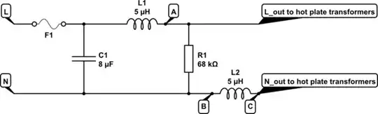
simulate this circuit – Schematic created using CircuitLab

(Note: R1 might also be 51kOhm (color codes are damaged), L1&L2 are 20.5 turns on a 1 inch yellow core.)

Description of Damage:

  • The PCB between the right terminal of L1 (point A on the schematic) and somewhere from L2 (points B or C alternatively, hard to say with a torroid) is severely eroded from arcing.
  • The casing material of resistor R1 is cracked and slightly blackened but the resistor is not "exploded" as one would expect from a overloaded resistor. It seems possible that R1 was simply in the arc path between the two inductances.
  • That being said, the terminals of R1 are also blackened. (Maybe due to a "wandering" arc?)

Photograph of PCB: enter image description here Bottom of PCB is pristine.

Questions:

  1. Am I right to assume that R1 has no function other than to provide a safe discharge path for C1 e.g. when unplugged?
  2. If so, why is R1 not directly parallel to C1? It seems like an odd design choice to run the discharge through L1...
  3. Any idea what caused the arcing (presumably between the two inductor terminals)?

My gut reaction:

My gut reaction is that there is no real issue with the filter PCB itself, but that a problem from down the line only manifests here.

Since induction hot plates work with high-frequency, is it reasonable to think that a fault with the HF part sends HF back up the line? If so, with HF being blocked by L1 and L2 it jumps between points A and C.

I am surprised, however, that a gap of about 10 mm can be bridged which seems to suggest an unexpectedly high voltage.

(Note: down the line a 1200V (visually undamaged) capacitor is used in the HF part of the hot plate which suggests the maximum voltage that should occur is the circuit...)

Null
  • 3
  • 3
ARF
  • 5,169
  • 9
  • 42
  • 69
  • This question seems to be aquiring votes to close. It would be great if those voting to close would give guidance on improving the question. – ARF Oct 08 '14 at 22:14
  • 2
    @ARF The votes to close are because it's a repair question. (I didn't vote to close it.) Although it's about repairing something, I think it is on-topic: The close reason text states: "Questions on the repair of [...] devices must involve specific troubleshooting steps and ***demonstrate a good understanding of the underlying design of the device being repaired.***" Clearly your question meets this criteria. – JYelton Oct 08 '14 at 23:01
  • +1 it's fine by me. C1 is the big black thing? 120 or 230Vac? It looks like just the resistor let go. What happens in the event of a HV pulse on the power line? – George Herold Oct 09 '14 at 00:06
  • @JYelton I'd recommend reading the question again. It isn't a repair question, the OP is wondering WHY it failed or rather possible failure mechanisms/paths. – placeholder Oct 09 '14 at 01:00
  • 1
    @placeholder Understanding failures is an important part of design, is it not? I don't see how this question fails to meet on-topic criteria. – JYelton Oct 09 '14 at 01:05
  • @JYelton Huh? You've got me confused, here is a quote from your comment "The votes to close are because it's a repair question...." now you are saying it's isn't? I'm saying this is a perfectly fine question, and indeed understanding failures _**IS**_ important. – placeholder Oct 09 '14 at 01:09
  • @placeholder Oh. I thought you were trying to say it should be closed for some reason. Sorry. Per your comment, I agree it's not strictly about repair, but the distinction between failure analysis and repair is fairly minor IMO. – JYelton Oct 09 '14 at 01:11
  • @GeorgeHerold Yes C1 it the black thing. It's a MKP 8µF+-5% 275V~ (400DV). I cannot exclude the resistor as origin of the arcing but the damage does not seem consistent with this: i.e. unexploded resistor and arcing signs on the terminals of the inductances. Are you suggesting I am putting a HV pulse on the power line to diagnose or asking if I understand how the filter reacts to it in theory? - My gut reaction is that there is nothing wrong with the filter circuit per se but that something down the line is causing the problem that just happens to manifest here. Is this possible/likely? – ARF Oct 09 '14 at 08:09
  • @JYelton Thanks for the hint. I think this might be because the original title suggested it was a repair question while the body of the question focussed on analysis. I have changed this which seems to be what people were objecting to since no more votes to close have been cast since. – ARF Oct 09 '14 at 08:14
  • Was it humid the day it failed? Or had you spilled water nearby? That's a paper-phenolic PCB, and if you had surface contamination/condensation, you could have flashover because the creepage distance was not sufficient for the pollution level. – Connor Wolf Oct 09 '14 at 09:01

2 Answers2

1

I believe that what happened was a combination of the resistor overheating (due to reflected RF), causing the air between the inductors to become more easily ionized, which caused the RF to arc across the inductors, heating the resistor even more, and the cycle repeats until something "gives."

Guill
  • 2,430
  • 10
  • 6
1

During the arcing period in the distribution board, the inductance and the capacitance of the active circuit creates the high voltage pulse with high frequency ( f=1/t) f= frequency of the pulse, t= time for the change in current ( Due to arc and operation of IGBT switching ). This high voltage pulse is affecting the R1 resistor. The gap between the R1 resister is around 10mm only this area is having the less dielectric strength compared to other places in the PCB ( due to through hole mounting of components the dielectric strength of the PCB reduces ) so, breakdown of solid dielectric ( PCB) ha pend. The R1 resistor is not only used for discharging of C1, but it also act as a damping resistor for transient voltages.