8

I'm currently laying out a PCB in eagle for a circuit that will form the basis for some experimentation. Instead of adding a row of headers so that I can plug it into a breadboard, I figured I would try and layout a small protoboard directly onto the PCB itself. I have room to spare on the board and the resulting creations will be somewhat more resilient. This PCB is a good example of what I'm shooting for.

I have considered using vias, but I seem to recall they are usually sealed off with a chemical to prevent solder from bonding. This is obviously not what I'm going for. Adding hundreds of single-pad components to my schematic does not seem very appealing either.

What is the best way of achieving this using Eagle?

EDIT: Thanks for your help everyone. Here's the design and here's the finished product.

enter image description here

drxzcl
  • 3,735
  • 2
  • 30
  • 32
  • 2
    you can't just place pads freehand in Eagle? Every piece of PCB software I have used has let you place primitives in the PCB design stage without having to have analogous schematic entities, they just don't have nets (which isn't important here, anyways). – Connor Wolf Apr 19 '11 at 05:16
  • 1
    I've searched around a bit and I have not found a way to place pads free-hand (yet), but that does not mean it's not there. If I try to drop, say, a 1x1 connector it tells me I should be making changes in the schematic instead. It's my first non-toy PCB projects, so I'm learning as I go along. – drxzcl Apr 19 '11 at 06:56

6 Answers6

6

You could use the 1x25 package in the SparkFun Eagle library as a starting point. It gives you 25 pins spaced 0.1" apart (used for single row headers). Modify to taste.

enter image description here

tcrosley
  • 47,708
  • 5
  • 97
  • 161
  • I would be there is probably a part for 2x25 as well. – Kellenjb Apr 18 '11 at 23:45
  • 2x8, 2x10, 2x12, and 2x26 -- but no 2x25 :) It would easy to modify any of these using cut and paste to create a larger array, e.g. 10x50 – tcrosley Apr 18 '11 at 23:53
  • Just to be clear, when you say "modify to taste", do you mean to modify it in the library or in the PCB editor? – drxzcl Apr 19 '11 at 06:57
  • 1
    I meant creating a custom version in the library for your own needs, using this as a starting point. There are several tutorials around on this topic; just Google: modifying eagle cad library – tcrosley Apr 19 '11 at 08:18
5

At some point, with any EDA tool, you're probably going to have to create a custom part for something; so you might as well dive in and create a proto-area part with an array of pads the way you want. You need to make the schematic component for that as well and place it on your schematic.

This is a good technique also for design-specific holes, especially if the holes have to align to some externally defined dimensions. Having a pseudo-component in your schematic to call out those features would make those features "official" parts of your design.

Toybuilder
  • 2,018
  • 1
  • 11
  • 12
  • I created a part with the pads in the proper places, and I'm happy to report it was easier than I thought it would be. Having troubles connecting the pads though (I'd like to make a few islands, as well as 5V and GND rails). The saga continues. – drxzcl Apr 19 '11 at 19:48
  • In your schematic component, wire the appropriate "pins" to the Vcc and ground nets. Or, better yet, wire them to "proto_vcc" and "proto_gnd" nets, separate from the main vcc and gnd nets. – Toybuilder Apr 19 '11 at 20:12
  • When trying to connect the pads with wires in the package editor, I rack up tons of "Overlap" DRC errors. I read in the Eagle forums that it's a known problem: can't change the name of wires in teh package editor, so Eagle does not know they are supposed to be the same connection. Oh joy. – drxzcl Apr 20 '11 at 20:18
  • What I'm suggesting (and I haven't used Eagle in like a decade so I'm only talking about general principals here) is to leave the pad area component unwired. Instead, make the bare component with only the pins/pads, and then wire them as appropriate in the schematic and pcb editors. – Toybuilder Apr 20 '11 at 20:31
4

There is a thread on the Eagle Support forums that deals with this issue in detail. One of the replies includes a link to a library of prototyping components.

drxzcl
  • 3,735
  • 2
  • 30
  • 32
4

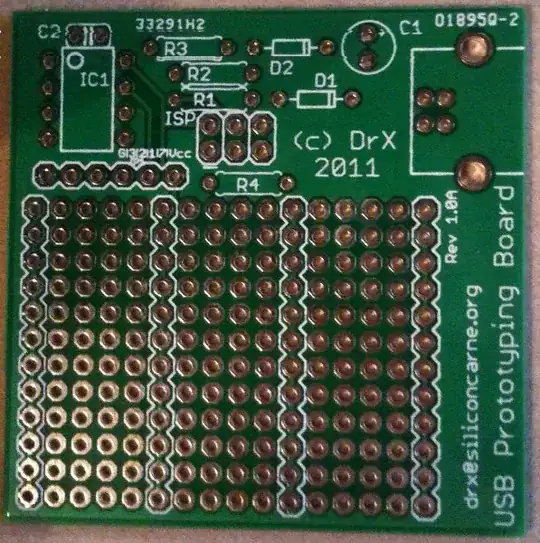
EAGLE trains you to add schematic parts for everything that appears on the PCB, but in this particular case, you really want to just add the holes, traces and silkscreen elements directly to the PCB. Think of it more as technical drawing than building a circuit.

I did this in the spare space in the upper left corner of my PIMETA v2 board:

PIMETA v2 board layout

The holes are 40 mil drill with 70 mil pads, and the traces are 40 mil.

I highly recommend adding silkscreen outlines, as you see above. This makes clear which pads are connected to which. That was particularly helpful on this board, since the traces were on the bottom, but even if they were on top, I'd add the outlines. The contrast of silk on solder mask is simply a lot better than for the copper under the mask.

Most of the pattern is intended to support DIP chips. The bits at the leftmost edge deviate from that partly due to lack of space but also to support an optional switch. (That's the translucent yellow overlay you see.) It's not important, here, to discuss what those switch pads are good for. The point is that you may not want to make your prototyping area completely generic. You should think through the scenarios of how the prototyping area will be used, and if there are special features you can add that will make it more useful than a generic protoboard pattern, do so.

Another example where I deviated from generic patterns is that some of the pads connect to the board's existing power and ground rails: V+, V-, B+ and IG. Doing that is one of the major advantages of having a prototyping areas on a special-purpose PCB, as opposed to using generic off-the-shelf protoboard: it means that things built up in the prototyping area can be run directly off the board's existing power supply and you don't have to run hookup wires across the board to get back to power points elsewhere. I recommend that you do the same.

Warren Young
  • 3,742
  • 24
  • 30
  • When trying to connect the pads with wires in the package editor, I rack up tons of "Overlap" DRC errors. I read in the Eagle forums that it's a known problem (can't change the name of wires in teh package editor, so Eagle does not know they are supposed to be the same connection). The PCB house requires a clean DRC. Any suggestions? – drxzcl Apr 19 '11 at 19:48
  • Don't use the package editor for this. Draw directly on the PCB itself. Use the VIA command for the pads/holes, and the WIRE command to connect them. You can use WIRE to draw the silkscreen outlines as well. I just tried it, and it passes the default DRC settings, at least. – Warren Young Apr 19 '11 at 22:19
2

What you are talking about with regards to the vias is solder mask capping them. In most good PCB programs you can get rid of the solder mask over a via by expanding the hole cut in the mask. This thread seems to be useful.

Thomas O
  • 31,546
  • 57
  • 182
  • 320
  • Yes, I was indeed talking about the solder mask. Thanks for the useful link. If I understand it correctly by placing polygons over the top/bottom of the vias in the t_stop/b_stop layers I can force the vias' copper to be exposed. – drxzcl Apr 19 '11 at 06:59
  • @Ranieri, I don't use Eagle so I wouldn't know, unfortunately. I would think there is an easier way. – Thomas O Apr 19 '11 at 11:36
2

I'm not acquainted with Eagle, but I guess it has copy/paste like any EDA program. Set your grid to 0.1", place a free pad, copy and paste. Select both pads, copy/paste. Select all four pads, copy/paste. You can do the whole area in less than a minute.
Vias are a bad choice because 1) they're too small, or you'd have to make a custom one, and 2) the pad of a via usually has a solder mask, which you would have to remove.

stevenvh
  • 145,145
  • 21
  • 455
  • 667