39

What is the reason that most of ICs (e.g. MCU) has multiple (A/D)GND and (A)VCC pins?

If it is to increase performance of an IC, how does it help to performance? or is it easier for the IC designer to connect some pins externally?

some footprint of ICs have a GND connection under the case, how does it help? Would it improve performance of an IC if I draw a GND under the case even if it is not required?

Angs
  • 3,275
  • 8
  • 33
  • 54
  • For example, [this 3-state buffer IC](https://www.ti.com/lit/ds/symlink/74ac11244.pdf?ts=1643067189457&ref_url=https%253A%252F%252Fwww.startpage.com%252F). Do I have to connect __all__ the `VCC`s to (e.g.) +5V and __all__ the `GND`s to (e.g.) 0V ? – LRDPRDX Jan 29 '22 at 09:16

4 Answers4

44

Three reasons come to mind:

1) Take a look at this close-up of the guts of a microcontroller. enter image description here

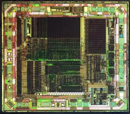
There's a LOT going on in there. And every part of that die needs power. Power coming in from any one pin will probably have to snake it's away around a lot of stuff to get to every part of the device. Multiple power lines gives the device multiple avenues to pull power from, which keeps the voltage from dipping as much during high current events.

2) Sometimes the different power pins supply specific peripherals within the chip. This is done when certain peripherals need as clean a voltage supply as possible to operate correctly. If the peripherals share the power supply that the rest of the chip uses, it may be subject to noise on the line and voltage dips. An example is the analog power supply. You noticed it's typical to see an AVCC pin on MCUs. That pin is a dedicated supply just for the analog peripherals on the chip. Really, this is just an extension of #1 above.

3) It's not uncommon for an MCU to power its core at one voltage but operate peripherals at another. For example, an ARM chip I worked with recently used 1.8V for its core. However, the digital output pins would supply 3.3V when driven high. Therefore, the chip required a 1.8V supply and a separate 3.3V supply.

The main thing to remember is that all of those supply pins are absultely necessary to connect. They are not optional, even when doing development work.

As for the bottom pad on the chip, it's there for extra heat sinking. The chip designer decided that the casing and pins of the chip may not sink the heat away from the silicon enough. So the extra pad on the bottom acts like a heat sink to help keep the temperature down. If the part is expected to need to dissipate a lot of heat, you'd want to have a large copper pour to solder that pad onto.

Dan Laks
  • 8,504
  • 4
  • 27
  • 43
16

There are three main reasons to require multiple power and ground pins.

  1. Impedance. Chips can draw a lot of current. CMOS chips in particular (basically any modern digital IC) draw huge amounts of current for very short periods of time on every clock cycle. Any impedance (in this case resistance or inductance) in the supply connection will result in voltage variations or voltage droop in the chip's power distribution network. This can cause problems with reliable operation. This is also why bypass capacitors are used; they prevent these switching transients from affecting other components on the board through the power rails by providing a return path for the high-frequency currents very close to the chip. Large chips actually place bypass capacitors directly on the package. If you look at a modern CPU, you can see bypass capacitors soldered to the package around the chip die and/or on the bottom if there is a hole in the pinout. The best place to put them would be on the die itself, but capacitors take up a lot of silicon area and therefore this is too expensive to be feasible in most cases. Separate analog supply pins are used to prevent switching noise from the digital portion of the chip from affecting the analog portion of the supply via the impedance of the pin and/or bond wire. Multiple supply pins are also required for chips that consume very large amounts of current. A modern microprocessor can consume around 100 A at around 1 volt. The resistance of the supply wiring must be very low, otherwise there will be a very significant amount lost to heat. In some cases half of the hundreds or thousands of pins on the chip will be power and ground pins in order to get a low enough resistance in the power and ground paths.

  2. Multiple voltage requirements. Sometimes different portions of a chip will run at different voltages. A classic example is a low voltage core and high voltage I/O. The core uses a lower voltage to reduce power consumption (power consumption in CMOS is more or less proportional to frequency and to the square of the voltage, so if you can lower the voltage by 30 percent you can get a 50 percent reduction in power) while the I/O runs at a higher voltage in order to interface better with external circuitry. Sometimes the core voltage is even variable. This is done in a power optimization technique called dynamic voltage and frequency scaling (DVFS). As the software load on the chip changes, it will command the frequency and voltage to change to save power. When the frequency is lowered, the voltage can also be lowered to achieve a 'triple whammy' power savings - lower frequency means lower dynamic power (proportional to frequency), and lower voltage means both lower static (proportional to voltage) and lower dynamic (proportional to voltage squared) power.

  3. Signal integrity requirements. In modern chips, signals on pins can transition very quickly. The current required by these transitions require a return path through a power or a ground pin. If this pin is far away, it ends up creating a rather large inductive loop that not only affects the power/ground pin and the signal pin in question, but also any other pins in the loop due to the magnetic field. This results in crosstalk where one signal affects adjacent signals. Chips have to be designed not only with enough power and ground pins to supply power, but also with pins in reasonable locations to reduce crosstalk.

Xilinx created a particular power and ground pinout scheme called sparse chevron. The idea is to create a patten of power and ground pins that place return paths as close as possible to all of the I/O pins, while not requiring an insane number of power and ground pins. The figure below represents all of the power and ground pins on a Virtex 4 FPGA in a BGA package with 1513 pins.

Virtex 4 FF1513 power pinout

The high concentration of Vccint and ground pins in the center supplies the core voltage to the actual FPGA die. The FPGA can draw up to 30 or 40 amps at 1.2 volts. The high number of pins is required to provide a low impedance path for the high current supply to the programmable logic array. The Vccaux pins supply power to some supporting circuitry, including the JTAG interface. The pattern of Vcco and ground pins supply power to the I/O banks. They also provide return paths for the actual I/O signals. Every I/O pin is adjacent to at least one power or ground pin, minimizing the inductance and therefore the generated crosstalk.

Some FPGAs also incorporate high speed transceivers that can be as fast as 28 gigabits per second. The high speed serializers and deserializers are basically very high speed analog circuitry (one you get to a high enough speed, nothing is really digital anymore) and so they need dedicated supplies. Generally these are supplied with separate linear regulators to ensure that this sensitive circuitry operates correctly and to ensure the many GHz worth of transients do not adversely affect anything else.

alex.forencich
  • 40,694
  • 1
  • 68
  • 109
14

The reason for separate Analog and Digital VCC and Ground is to separate and keep the rails clean. Analog inputs are sensitive to digital noise.

The reason for multiple external grounds can be due to internal wiring efficiency. Sometimes its not practical to route a ground internally on the IC wafer. But another reason is heat dissipation. Multiple ground pins, including the GND connections under the case, are used to ensure more thermal conductivity to the PCB the IC is connected to.

Passerby
  • 72,580
  • 7
  • 90
  • 202
8

Also, drawing lots of current may be impractical on one pin alone. Think about resistance: those wires are very thin and can't carry to much current.

Thus, a more complex µC spreads its load requirement over many pins. This is also often the reason why cables carry two or more powered lines, e.g. Power-over-Ethernet.

riot
  • 81
  • 2