1

I thought the conventional method to denote the direction of the bias current is to precede the IIB parameters with the '+' or '-' flag in the 'electrical characteristic' table, '+' indicate the bias current flows into the terminal, and '-' indicate the bias current flows out the terminal. Just like the Op amp LM358.

But recently i find the datasheet of comparator LM311 is difference. I note it have PNP input stage, but the IIB has no '-' flag.

I want to know:

  1. LM311's input bias current does flow out of the terminal, am i right ?
  2. If i am right, why LM311's datasheet is different from Op amp's ? If it means the 'conventional method' doesn't apply to comparator ?

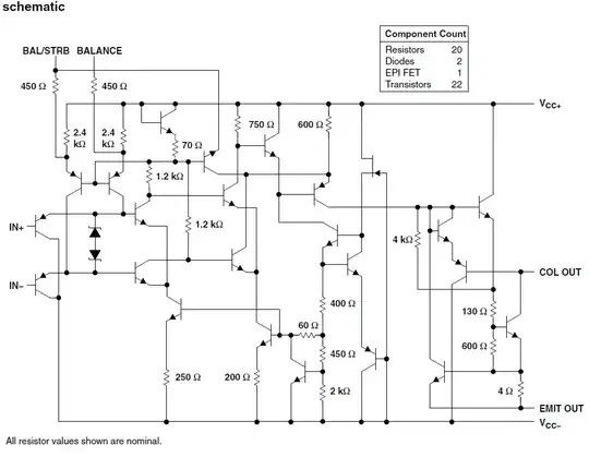
The schematic from LM311's datasheet:

enter image description here

diverger
  • 5,828
  • 5
  • 43
  • 79

2 Answers2

1
  1. Yes, the LM311's input bias current does flow out of the pins - the schematic on page 3 of the data sheet shows PNP transistors and this implies bias current flows from the pins.
  2. Yes, the LM358 data sheet shows this current as a negative current but, the bias current will be flowing out from the pins just like the LM311.

Some op-amps, notably rail-to-rail input op-amps may specify this as "+/-" because they usually have NPN and PNP combined input stages. But if one of two (or maybe plenty) of data sheets don't obey the convention I don't think it's a big deal - if you have to deal with bias currents (on sensitive applications) you match the input resistances or use low enough resistances around the inputs to minimize the effect. What will remain is the input offset current which can always be presumed to be "+/-" because one input's bias current may be slightly less or more than the other input's bias current.

Andy aka
  • 434,556
  • 28
  • 351
  • 777
0

The polarity of the Input Bias current can't simply be derived from the simplified schematics in the data-sheet. Often the implementation internally is very different than what is shown. Parasitic elements are not shown for example, which may be the dominant (in this case) mechanisms for leakage current.

Second order effects, like dealing with leakage current is very important for getting the desired results and doing a complete design in op=amp applications. There is one assumption that you must make, which isn't explicitly stated in any datasheet; that the input structures are laid out in such a way that they are as matched as possible. In fact if the designer (layout wise) does not do the layout for matching the chances are that the device will probably have very low yield). I couch my terms here using "probably" simply because I don't want to pretend that I know how ALL designs flow, I can imagine some designs and have had some experience where this is violated intentionally. But this matching assumption applies in most cases.

So what you need to do is, make sure that your external circuitry is also as matched as possible. That means that the input resistance for the + and - terminals are the same so that when the "matched" leakage currents interact with the external components that the common mode voltage generated shifts in the same direction together (remember that the input stage is a differencing circuit.

This philosophy applies to matching the TCR (Temperature coefficient of resistance) and indeed for really precise designs one typically aligns the external components like resistors in the same direction (Ideally - across the thermal gradient on the board - but it is more important that the direction match). In fact this is one of the things I look for in a design review of a PCB "Has the layout taken into account factors to ensure that the components experience the same conditions?".

So the sign of the \$I_IB\$ is less important that the magnitude of the effect so be taken into account of with the error budget of the design. In other words, keep things symmetrical and don't worry about the sign.
placeholder
  • 29,982
  • 10
  • 63
  • 110
  • thanks for your answer, but i don't mean the '+' and '-' terminals on the schematics, i mean the IIB parameters in the 'electrical characteristics' table. – diverger Aug 23 '14 at 10:40
  • That those + and - are not "flags" or labels they are the actual values. Why would you call them flags? – placeholder Aug 23 '14 at 10:45
  • yes maybe it's a mathematical problem whether the '+', '-' should be a part of the actual value, but here they did have a practical usage here: the '+' and '-' denote the flow of the current, so i split them from the actual digits. I think you've understand my question now, :). – diverger Aug 23 '14 at 10:51
  • I've appended the schematic from the LM311's datasheet, i think it's not so 'simplified'. It has PNP input stage, and i think the bias current should flow out of the terminals, but the IIB parameter doesn't have '-'. – diverger Aug 23 '14 at 10:55
  • @diverger and you "know" this because of what precisely? Do you how the transistors are laid out on the substrate? do you know the relative areas of the base to Emitter vs. base to collector?. Where are the parasitics devices in that drawing? – placeholder Aug 23 '14 at 14:54
  • No, i've no way to know the details including parastics from the schematic, but i think they should show the 'important' part in there datasheet. So i went to the electrical characteristic table, from the electrical characteristic table, if it 'obeys' the convertional, the bias current should flow into the terminals, but if judges from the schematic barely ( it didn't show any thing parasitics right ? Am i wrong ? ), it should flow out of the terminals. I'm not sure which one is right, so i ask for help here. Then what's your opinion ? Can your give me a answer ? – diverger Aug 23 '14 at 17:03
  • @diverger new edits for clarifiaction – placeholder Aug 23 '14 at 18:28