I need pads with holes in by PCB, but the top and bottom side of the pads need to have different nets i.e. the top and bottom sides must be isolated. Here is the picture 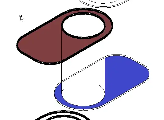
Is this possible to fabricate for the PCB manufacturers? If yes, how do I design this in Altium?
Asked
Active
Viewed 1,872 times
11
zud
- 1,746
- 6
- 25
- 42
-
Interesting question. If you were to make your own double sided PCB, this would be the default state - vias not plated through. I believe it's the hole drill order. Drill X holes, then plate, then drill the remaining. – carveone Aug 21 '14 at 14:05
-
@carveone But vias have pads with same net in all layers, this one does not. – venny Aug 21 '14 at 14:07
-
Yes. That's true - you would get errors by doing that. I was just thinking about the manufacturing process more than the PCB design process! – carveone Aug 21 '14 at 14:11
-
2I've reread the question a few times, and see what you're wanting. What exactly is the point of doing this? – Matt Young Aug 21 '14 at 14:14
-
@MattYoung Many coaxial wires in small area – zud Aug 21 '14 at 14:22
-
1It sounds like you're planning to solder the shield to one side of the board and the inner conductor to the other, which basically sounds like an assembly (and reliability) nightmare. Have you considered simply bringing the pads to the edge of the board (no holes) and soldering them there? I have actually seen something like this done in certain cable assemblies. – Dave Tweed Aug 21 '14 at 14:48
-
@DaveTweed You are right. But I have many rows of pads. I cannot bring all the pads to the edge. Thanks for the suggestion though – zud Aug 21 '14 at 14:57
-
@DaveTweed - Not so. This can be a very reliable way to attach wires to a space constrained PCB. We often use a via that snugly fits the wire insulation, poke the wire through, and solder it on the other side. Pretty robust. – Rocketmagnet Aug 21 '14 at 14:59
4 Answers
10
I don't see any reason why you can't create a footprint with overlayed pads on top and bottom going to different pins. Just specify the hole as unplated. If you avoid drilling one of the holes (make it an SMT pad) you may be able to avoid all DRC errors with little fuss (otherwise it may complain that the two drilled holes have insufficient clearance).
Altium definitely understands that pads on top of each other separated by an unplated hole are not connected.
Edit: It only seems to understand this when the unplated hole is part of a single pad. Otherwise it thinks they are connected, even with an unplated hole.
I tried this with a simple pad on the top and a multilayer on the bottom, unplated hole and padstack edited to have copper only on the bottom and there is still a short circuit error in the DRC check, despite the unplated hole. The 3D view shows that the copper is not there, so Altium's DRC is not picking up on it.
Spehro Pefhany
- 376,485
- 21
- 320
- 842
-
1Regarding your fab question, there may be some that don't do unplated holes or charge a premium, but all the places I deal with have no problem with it. The default for the output job is to combine both hole types in a single drill file with comments ;TYPE=PLATED and ;TYPE=NON_PLATED in the tool list. – Spehro Pefhany Aug 21 '14 at 15:55
-
Yes, I will ask the PCB mfr. before ordering. For the footprint, I placed SMD pads on top and bottom layers and placed a hole on them. Now I get _Short-circuit Constraint_ and _Clearance Constraint_ errors in DRC between the pads and the hole. Can I ignore these errors? – zud Aug 21 '14 at 16:54
-
1I think you should change the rules to make the errors go away except for a possible warning of unplated holes. There is some weirdness associated with this kind of thing- the polygon pours don't like it, for example. Take extreme caution and look at the Gerber files and 3D view before sending it off would be my advice.. – Spehro Pefhany Aug 21 '14 at 17:49
-
Okay, another thought came to me- making the component a "net tie" (in the schematic symbol) marks it so that the only DRC comment is a warning about unverified net ties (no errors). Autoroute even works. However, polygon pours still improperly avoid the pads, so caution is called for. – Spehro Pefhany Aug 23 '14 at 02:24
4
In addition to the other answers, regardless of what you can do in your software, you may have trouble when you go to have your board fabbed. Some shops interpret copper at the edge of, or under a hole as being a plated hole. OSHPark for example does things that way. You'll have to be careful to ensure that the copper layers don't intersect the edges of the hole, and leave a teensy tiny margin.
If the fab has a different system of indicating which wholes are plated and which aren't, then you're home free.
Otherwise, you could put a hole much smaller than what you need in the spot, ignore the plating, and ream it out up to size yourself.
whatsisname
- 1,434
- 1
- 10
- 16
2
I'll add that in Eagle you can add mounting holes which have no electrical connection between the different layers in a board or in a package.
HOLE - Function Add drill hole to a board or package.
Board houses can do this but you should check with them before ordering.
carveone
- 2,568
- 1
- 15
- 22
1
That is basically an unplated hole drilled through two suface-mount pads. Yes, it is possible to fabricate but may be for additional cost, because it is done in separate manufacturing step. From what i have seen this will leave bare copper on sides of the hole (not a big deal).
In Altium, it will probably cause DRC errors which you can ignore.
venny
- 3,058
- 13
- 16