In Decoupling caps, PCB layout, three variants of placing bypass caps are presented:
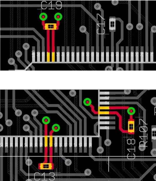
In the comments, it is mentioned that C19 is the worst approach, C18 slightly better and C13 the best way, which is somewhat contrary to my understanding, so I'd like some clarification.
I'd expect the C19 layout to be close to optimal:
- the capacitor is placed in-line between the vias to the supply planes, so high-frequency components can be filtered out optimally
- the vias are not too far apart
I'd probably use wider traces between the capacitor and the vias (Altera's AN574 suggests that).
C13 is a bit closer to the IC, but the vias are on the far end of the connection, so I'd expect worse behavior at high frequencies (probably too high to matter, but...)
The C18 layout is the worst:
- the vias are far apart, increasing inductive impedance
- the loop is fairly large
- same issues as C13 with high frequency ripple
Where am I going wrong with my analysis?