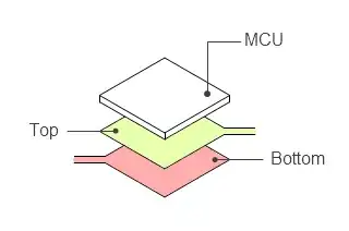
As you know most of the MCU's has several Vdd and Vss pins. In the case of two-layer PCB it seems convenient to use some polygons beneath MCU (like on the figure below). The first option is treat the top polygon as a ground and bottom as a power. The second option is treat the top polygon as a power and bottom as a ground. There is a third option: don't use two polygons and route power or ground by individual traces even though it's not very easy.
So which options is preferable in terms of a better chance of a good prognosis? Maybe there are other options?