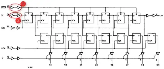
I would add to Sphero's very good answer that you should not take these IC internal diagrams literally. They are intended to show essential internal functionality, but not necessarily detailed internal structure.
For example, do the D-Flops on the silicon actually have a low-going RESET input as indicated by the diagram? Maybe, maybe not.
Does a low-going pulse on the IC's SCLR- pin clear the IC's Q output pins to Logic 0 (assuming the outputs are enabled by G- pin being held low)? Yes. Does that mean that the internal flops actually utilize their Q output driving a non-inverting output buffer as shown? Or, do the internal flops actually use their Q- outputs and an INVERTING buffer? Either topology is possible and you will never know which is the case as an outside observer.
There are a lot of shortcuts and silicon magic performed in all ICs which is not always easily portrayable in a conventional schematic diagram. Remember, the IC is not made up of individual gates, but transistors. If the manufacturer gave the schematic of the actual transistor circuitry etched into the chip, users would know the exact nature of the internal circuitry, but be deprived of a concise diagram of essential functionality of the chip. That's what these diagrams are meant to portray - essential functionality.