What is the meaning of biasing in electrical/electronics circuits? What is the need for biasing in BJT/MOSFET? What will happen after biasing when we apply input signal(AC/DC)? Will biasing signal and input signal superimpose?
Asked
Active
Viewed 3,574 times
0
-
It depends on the context. If you are designing an *amplifier* then you want to bias the output such that it has equal "room" (it's known as voltage *swing*) for the superimposed AC signal to propagate without clipping. For instance you cannot generate a neative collector voltage with an NPN transistor, so you must bais it with DC and decouple the output with a cap. Or perhaps you have an AC signal that you want to measure using an ADC. Since common ADC cannot measure negative voltages you have a problem unless you bias the signal such that during the negative cycle it does not go below zero. – sherrellbc Jul 08 '14 at 12:25
-
Sir, I can't understand the biasing meaning...please explain little more... – Deepak Berwal Jul 08 '14 at 12:39
1 Answers
2
Your question is ambiguous, but I will answer one possible case, namely, "Why might someone apply a DC bias to a BJT?".
An NPN BJT does not conduct very much current when the base-to-emitter voltage (Vbe) is less than 0.7V. Typically, a base biasing network for a BJT is used to bring the base into the 'forward active region', where changes in voltage at the base translate into changes in current into the collector of the device.
A thought experiment: 1) An AC signal (lets say, 100mVp-p sine wave) is applied to the base of a BJT through a capacitor. Nothing else is connected to the base of the transistor, the emitter is connected to ground, and the collector is connected to the positive power rail (lets call it 3.3V) through a 1k resistor. The collector voltage won't change as the sine wave at the base is applied.
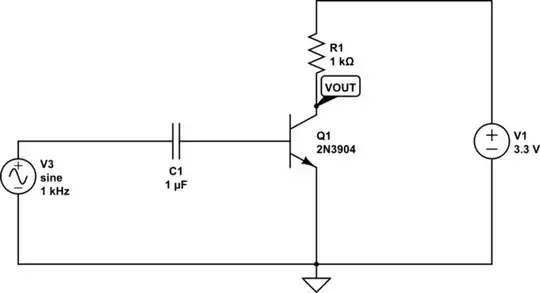
simulate this circuit – Schematic created using CircuitLab
2) Now, imagine the same circuit, except that there is a base biasing network above 0.7V. The output voltage (Vout) will now be changed as the input voltage changes, since the BJT base is above the "cut-in" voltage (approx 600-700mV for silicon BJTs).
There are plenty of other considerations regarding temperature dependence, quiescent current, and input and output impedance of the circuit, among others. I'm just attempting to get you to a basic concept of one type of DC biasing.
I haven't had time to test out the circuits provided, they are just for conceptual use ...
Most of this information is excerpted from Wikipedia and allaboutcircuits: http://www.allaboutcircuits.com/vol_3/chpt_4/10.html http://en.wikipedia.org/wiki/Bipolar_junction_transistor#Regions_of_operation
jjmilburn
- 427
- 3
- 10