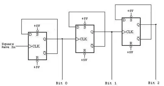
This is a ripple counter:
simulate this circuit – Schematic created using CircuitLab
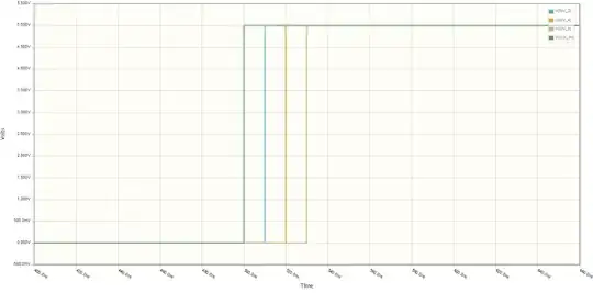
It is an asynchronous counter that will divide the input clock by 2 each stage. It is an asynchronous counter because each stage will change at different times and each flip-flop has a different clock input. The time difference between each stage is determined by the CLOCK->Q delay of the flip-flop used. The simulated result is shown below, showing that each stage delays the output transition by the clock-to-output delay.
Now to put the significance of this in perspective of an FPGA, the timing analysis tool wants to make sure everything is getting clocked at the right time. Part of that is make every signal that enters the CLK pin of a flip-flop a system clock that should be synchronized with all the other clocks. As such, if I entered the above schematic into an FPGA synthesis tool, it would consider the nets CLK_IN, DIV_2, DIV_4, and DIV_8 to be "clock" nets regardless of whether they are used to drive any other clocks. This will probably work fine as a counter (there is a possibility for a hold-time violation on each flip-flop), but it's not made in the synchronous logic method.
If you're using this to take a fast input clock and derive a single, slower clock (e.g. make DIV_8 a master clock for the system) then you're probably fine.
The trouble comes in when you want to have fast circuits clocked with CLK_IN interacting with slow circuits clocked with DIV_8. In this case, you want the rising edges of the clock to be synchronized, but you will have a large clock skew between these clock nets. The amount of clock skew generated by one stage could be enough to cause synchronization errors, and more stages will almost guarantee it.
If you want to create two synchronized clocks inside an FPGA, your best bet is to use a synchronous clock generator, or a clock module that is internal to the FPGA, such as a PLL/DCM block.