9

How can I determine (estimate) maximum reasonable PWM frequency for 2SK2554 transistor?

I found timings in datasheet:

enter image description here

I could estimate frequency from this (and make sure that all these times are 20-50x shorter than my PWM cycle length or something like that. But I have Vgs is between 4-5V, my maximum current is 10A.

Im asking because I have slow PWM now (~1kHz), but want to know how fast my PWM can be without loosing too much power while switching.

My load is big lead-acid battery (charging) or resistive (discharging).


So far - I've done simulation with similar, a bit smaller transistor (2SK2553) because there was no 2SK2554 in my Multisim.

This is graph for Vgs = 4V.

enter image description here

How much time (in percent for example) my switching time can take from PWM cycle time?

Kamil
  • 5,926
  • 9
  • 43
  • 58
  • Well since you have less current through your drain these values are likely to be *upper* bounds, a good start is \$t_{d(off)}+t_f<\frac{T_{switching}}{100}\$. If you can measure the square wave and you don't need to produce this your best option is probably measuring it, or you can simulate it, manufacturers usually give away some pretty complicated device models. – Vladimir Cravero Jun 15 '14 at 16:50
  • Wait that's a mosfet, you can ignore the "upper bounds" part, sorry about that. – Vladimir Cravero Jun 15 '14 at 16:53
  • It's 2SK2554, there is no such part in my Multisim. I simulated 2SK2553 (similar, a bit smaller) transistor. Ill add screenshots in my question. – Kamil Jun 15 '14 at 16:59
  • Maybe you can find something on the manufacturer's website, I've seen many spice models on ti, ad, maxim and so on... No Multisim anyway. – Vladimir Cravero Jun 15 '14 at 17:00
  • @VladimirCravero Well, I'm pretty satisfied with that formula you wrote, you can add it as answer, just add legend what is td and tf. – Kamil Jun 15 '14 at 17:04

2 Answers2

11

The main factor determining the switching speed is not just the MOSFET itself, but the circuit in which you have it wired.

From the point of view of the gate (i.e., the PoV of your PWM signal), the MOSFET can be seen as a simple capacitor. The MOSFET is considered ON when the voltage across that capacitor is above the threshold voltage \$V_{th}\$ and off when below (it's more complex than that, but that's a simplified model for now).

So it basically boils down to how fast can you charge and discharge that capacitor.

The longer the capacitor takes to charge or discharge the longer the device will take to switch, and the more power will be dissipated during that switching period.

There is a very nice PDF document from International Rectifier which introduces you to the basics of MOSFETs. The section headed "Gate Charge" is a good read for this problem.

It can be simplified down to the standard RC formulae for calculating charge time of a capacitor \$\tau=R \times C\$ - the capacitance of the gate, multiplied by the resistance of the circuit portion charging or discharging the gate. For instance, if you are switching the gate through 100Ω and the gate has a capacitance of 7700pF the rise time would be \$100 × 7.7e-9 = 770ns\$ for 63.2% charge. Adjust that time to suit the exact threshold voltage and your drive voltage of course.

Say you have 8 bit PWM, that's a possible 256 values, so you need an absolute minimum of 770ns * 256 time slices for switching, which is 197.120µs, or an absolute maximum frequency of 5073Hz. I'd limit it to half that so as to ensure a minimum of one time slice of level drive between switch on and switch off.

Of course, that's only a rough value. If you read through that PDF and compare it to the values in the datasheet you may be able to come up with more accurate values.

Majenko
  • 55,955
  • 9
  • 105
  • 187
7

When a step hits a mosfet gate there is some delay before the mos is fully on. This must be taken into account if you don't want to end up with a MOS that spends most of its time turning on (off) instead of (non) conducting in its ideal states, i.e. "fully on" and "fully off".

When the steps arrive two things happen: the gate-source capacity must charge and the inversion region must form below the gate. There's a sort of "dead" delay, i.e. nothing happens, both on turn on and turn off, since when the charge on the gate is below or above a certain threshold no current (or all the possible current) can flow: that delay is the delay time.

The rise and fall times take in account the time the current needs to get to its maximum value, or zero, it's as if you were walking along the mos characteristics in the linear (triode) region.

While the delay times are probably pretty much constant the rise and falls times depend heavily on the gate voltage:

  • on turn on, the higher the target gate voltage, the lower the rise time
  • on turn off, the lower the starting gate voltage, the lower the fall time

Sometimes you drive the gate with a high voltage to turn it on rapidly, then go back to the minimum \$V_{GS}\$ that guarantees saturation so that the turn off will be faster too.

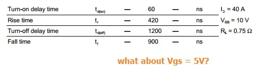
About your timings, I'd start summing the delay and the rise (fall) time for each transition:

$$t_{ON}=t_{d(on)}+t_r=480ns\\t_{OFF}=t_{d(off)}+t_f=2100ns$$

Let's assume you want to spend at most 1% of your time turning on or off your mos: you take \$t_{ON}+t_{OFF}=2580ns\$, multiply it by 100 and you have your period: 258000ns, or 258us, that is about 4kHz. In the comments I was simply neglecting the turn on time.

1% is a quite conservative limit anyway, it means that the wave really looks a square wave if you see it through a scope. You can probably go even a little higher and be safe, i.e. you are not dissipating much.

Vladimir Cravero
  • 16,007
  • 2
  • 38
  • 71