6

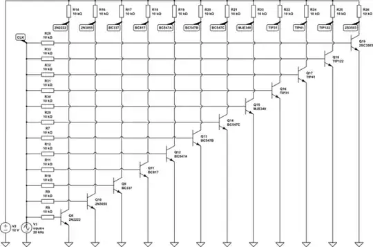
I did a test with randomly chosen 12 NPN BJTs. I applied a clock pulse to each of them and observed their collector voltages. Some of them showed very low rise time, while some responded terribly slow. As far as I realized, power transistors like 2N3055 yield very high rise times, while those which have very low collector current rating yield very low rise times.

I used to think that the "transition frequency" would give enough information about this. I chose a 100MHz transistor (BC817), but it couldn't survive even at 20kHz. Therefore, the "transition frequency" parameter shouldn't be giving enough information alone, or it should be about something totally different (I don't know).

My question is, how do I roughly predict step response characteristics of a BJT by looking at its datasheet? Which datasheet entries give information about this behavior?

schematic

enter image description here

hkBattousai
  • 13,913
  • 31
  • 114
  • 190
  • I think that is not a good test circuit. I'd use a current generator for each bjt so that each of them would go well deep in saturation region. – Vladimir Cravero Jun 04 '14 at 09:59

5 Answers5

7

It is usually capacitance that causes problems - and it's usually the miller capacitance that is the main culprit. The miller capacitance is internally from collector to base and if the base is driven from a high impedance (10k in your diagram - really quite high to expect decent performance) the miller capacitance forms a low pass filter with the input resistor.

If miller C is 10pF and input resistance is 10kohm then these two components form a low pass filter with a cut-off at: -

\$f_C = \dfrac{1}{2\pi R C}\$ = 1.59 MHz.

Try reducing the 10k ohm input resistor to something more sensible like 330 ohms and see the difference. I simulated a BC817 as you have drawn it and it took about 2.3us to reach 11 volts when switched off. With a 1k input resistor it took less 0.33us. With 330 ohms it took about 0.25us.

If I lowered the collector load to 1k and kept the 330 ohm input resistor it took about 0.09us.

The lowering of these resistors all serve to reduce the effect of miller capacitance (amongst other things).

Andy aka
  • 434,556
  • 28
  • 351
  • 777
4

In most datasheets there's a section named 'dynamic characteristics' or 'switching characterisics' (or both). There are also some parameters may be in 'small signal characteristics'.

Important parameters you should check are:

  • delay/rise/fall time -- they mean exactly they are: swithing times
  • current gain bandwidth product -- above this frequency part will not amplify at all (gain is less than one), at half frequency it will have gain of two etc.
  • input/output/etc. capacitances -- they affect circuit impedance, e.g. base resistor with input capacitance will form low-pass filter with specific cutoff frequency.

Note, if manufacturer designed transistor for linear mode then switching characteristics may be surprisingly bad. E. g. as you see transistor turn off time may be very long compared to turn on time. This is because lots of minor carriers in base area, which need significant time to recombine. This effect may be reduced e. g. by driving base with negative voltage when turn off.

Look and simulate schematic below to see how changing driving affect performance of switching

schematic

simulate this circuit – Schematic created using CircuitLab

Switching timing

Vovanium
  • 987
  • 8
  • 10
1

Internal capacitance is part of the problem as Andy and nidhin say. This affects the rise time component of the switching time, making a large high capacitance device like the 2N3055 slower than the BC547.

But several of the switching curves show something else going on : a long delay before switching starts; followed by a relatively fast rise time. These transistors are saturating : a quick glance at the schematic shows Ib=Ic (approx) and saturation is defined as Ib >= Ic*0.1.

Essentially, a saturating transistor stores charge in the base region, and when you remove base current, the remaining charge is attracted to the collector by Vce, but Vce is close to 0 so that attraction is weak, and the transistor remains conducting until the charge dissipates.

Fast switching transistors would be designed to minimise this charge storage.

This Q&A gives some of the back story on saturation and a possible fix, which might be interesting to try on one of the saturating transistors (e.g. green trace : BC337?) to see if its switching speed is improved.

0

I think its the internal capacitance which causes the delay. The rise time increases as these capacitance increases. I am not sure that all datasheets provides this data.

I have seen a few datasheets mentioning input capacitance and output capacitance (eg. BC547).

In circuitlab, the value for emitter junction capacitance (C_JE0) and collector junction capacitance(C_JC0) is given in the parameter of transistors. So may be you can compare the transistors used based on the capacitance values and hence make an inference because I am not 100% sure.

nidhin
  • 8,197
  • 3
  • 28
  • 46
0

Much will depend on the transistor. If the manufacturer expects that it will be used as you are using it, there will be a section of the data sheet labeled "Switching characteristics", which will consist of delay, storage, rise and fall times, plus the conditions under which they are specified.

If there is no such section in the data sheet, it's a pretty good bet that you don't want to use it for switching. In the case of the BC817, I have no idea why it behaves poorly. It has excellent saturation performance, and its gain-bandwidth product (also known as transition frequency) is about 1/3 that of a 2N3904 or 2N2222.

I can't read your graphs - text is too small, so I can't tell which trace belongs to which transistor.

WhatRoughBeast
  • 59,978
  • 2
  • 37
  • 97
  • "view Image" or your browser's equivalent allows you to expand the graph. –  Jun 04 '14 at 11:54