When routing a PCB, is it better to route a trace through a pad as in 1 below, or to route a pad to a trace as shown in 2 below?
When routing a PCB, is it better to route a trace through a pad as in 1 below, or to route a pad to a trace as shown in 2 below?
Electrically, there is no differences.
Well, in fact there are some... But only when considering very high frequency signals.
If the passive element is a decoupling capacitor, your solution 1 will looks like this:
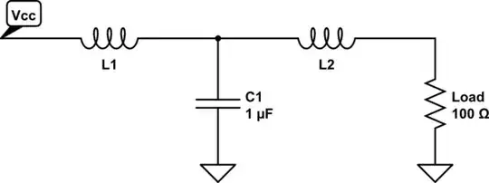
simulate this circuit – Schematic created using CircuitLab
L1 and L2 represent the little inductors made by the routing tracks themselves. You can see that the capacitor is connected directly between L1 and L2, without (or more precisely "negligible") inductance. The decoupling will be good. (even better if L2 is very small by putting your decoupling caps very close to the load).
But using routing option 2:
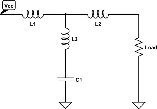
The little extra routing track forms an added inductor (L3) between the decoupling caps and the load. Thus your decoupling would be worse rejecting very high frequencies.
It worth nothing to mention that there is also an unwanted inductor at the GND connection of decoupling caps. This should be as small as possible too.
There is another reason: Reflow soldering.
Your component has to be "thematically balanced". I mean that your footprint has to look symmetrical. Thus it will heat-up evenly during reflow soldering and your component will not rotate or just move due to surface tensions into the liquid solder. Imagine that the solder paste get liquid on one pad when it is still solid on the other, because of thermal imbalance on the footprint: The component may move and end up soldered at one pad only. (see picture)
If both pads were routed using your option 1, this is not symmetrical in the X nor in the Y direction. But if both pads were routed using your option 2, this would have been perfectly symmetrical and this is good. In that point of view, everything that is symmetrical (in X and Y) is good. (there are other thing to consider but I will deliberately omit them here, because it would be out of scope)
I would finish by saying that these things are becoming critical only when considering mass production and relatively high quantities. Reaching thermal balance on your footprints may reduce by some percent the number of badly soldered components.
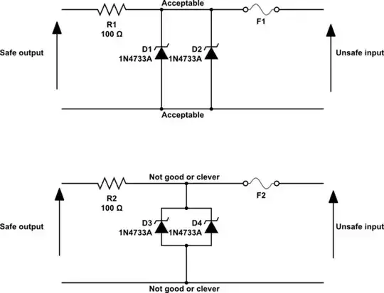
In the rather obscure field of designing zener barrier circuits (for intrinsically safe equipment), option 1 would be the preferred solution because if a zener diode became disconnected by a PCB track break, then the output of the "barrier" would naturally be disconnected from the potentially dangerous input voltage i.e. it is fail safe: -
simulate this circuit – Schematic created using CircuitLab
If you need to split a trace to two different locations, do it from the pad. I prefer option one, with one modification. Make each trace meet the the pad right on the corner. Personally, I like the nice smooth 135 degree pad to trace angle, but more importantly, having 45 degree angles between copper features is asking for etchant traps. Meaning that in the etching process, acid gets caught in the acute angle, and continues etching unpredictably. The boards will test fine in the manufacturing process, but there will be random failures in the field. The way to prevent it is keep all angles greater than or equal to 90 degrees. PCB manufacturers have better control over this than they once did, but for high reliability and long service life products, it's a chance not worth taking.
To add my E 0.01: For a prototype I prefer (for all other things the same) the 2nd option, because it makes it easier to cut the trace to the component and make some other connection to it. But when space is tight I will switch to the 1st version, although I would prefer to avoid that sharp angle.
I think that's quite personal (I prefer the second solution) but there are some objective differences. Option two might be better because soldering on that pad is somewhat easier since the thermal resistance to a bigger thermostat is double the first solution resistance. If you are soldering by hand that might make a big difference. Moreover excess solder can be swept easily away in solution 2, while in solution 1 that's somewhat more difficult. That's particularly true for SOIC or similar SMD chips, if your trace comes out at an angle it might be very, very difficult to solder them by hand.
I bet there are other issues, I'm sure somebody around here can add a lot, that's just my two cents. Anyway, as I said, I find option two a whole lot neater than one.
Simple, if its a POWER trace like VCC of GND you should defenetly go for 2, if its some signal its your choice.