1

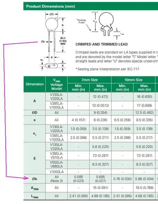
I am a new user of Altium Designer. I need to make a footprint of this varistor, and I cannot understand its drawing. Same thing happens for the rest of the components. Can someone here tell me how I am supposed to decide the pad diameter, height, width? Take this doc as a reference, and I hope I will cater other drawings as well then!

Here is the datasheet link (Littelfuse LA Varistor Series).

JYelton
  • 32,302
  • 33
  • 134
  • 249
alexhilton
  • 529
  • 2
  • 8
  • 16

2 Answers2

3

The datasheet describes a family of devices, which have similar shapes (disk with radial leads) but different dimensions. The case sizes are identified by the nominal diameter (even though a 7mm part can actually be as large as 9mm).

device family picture

To avoid making an individual drawing for each size, the authors of the datasheet made one parametrized drawing with letter designators, and listed the mechanical dimensions in the table below.

So for instance, the diameter of the pin is marked as Øb on the drawing. From the table we find that for 7mm size, will have pin diameter between 0.585mm and 0.685mm.

parametrized mechanical drawing
(p.10 in the datasheet)

Nick Alexeev
  • 37,739
  • 17
  • 97
  • 230
  • Great, that means the pad size will be between 0.585mm and 0.685mm? and what about the component height? It will be soldered so the height will be (15+4.69)mm? The two plus signs indicate what/ That they are non-polar? – alexhilton May 20 '14 at 18:08
  • @alexhilton the two plus signs indicate the center of the holes. – Cornelius May 20 '14 at 18:23
  • 2
    The hole size will be .685 mm, plus a bit, so you can easily push the wire leads through the holes. The pads will be somewhat larger. I'm accustomed to Imperial measurements, so I'd use a .035" hole in a .060" pad. The component height above the board is dimension "A": 12 mm for the 7mm size. You MUST learn to read these dimensioned drawings and the "version size" table - you'll find similar drawings and tables for many parts. – Peter Bennett May 20 '14 at 19:45
0

This is what you have to draw:

enter image description here

Dimensions are at page 10 of that datasheet. For information regarding pads/holes What pad hole (drill) size is appropriate for a given through-hole lead diameter?

Cornelius
  • 5,048
  • 4
  • 26
  • 45
  • I cannot understand the drawing, the link you posted says that you should know the specs from your board house! Also whats E and e? I am sorry I am being really dumb but that is the issue here I cant understand the drawing! – alexhilton May 20 '14 at 17:52
  • @alexhilton you set up a visible grid. _e_ is the horizontal distance between holes and _e1_ is the vertical distance. _E_ is not that important and it is no problem at all if you draw it a little bigger. – Cornelius May 20 '14 at 18:02
  • you mean e is the pitch? – alexhilton May 20 '14 at 18:09
  • @alexhilton yes, _e_ is the pitch. – Cornelius May 20 '14 at 18:12
  • Correct me if I am wrong. If I take 7mm disc then Atrim+Ltrim is the height, e is the pitch, the dia for the pads is between 0.585-0.685mm, and what else am I missing here to complete my design? – alexhilton May 20 '14 at 18:19
  • @alexhilton why do you care about height when designing a PCB footprint? Start by placing a pad, then move _e_ mm to the right and _e1_ mm up. Here place the other pad. Now draw that rounded rectangle around them. – Cornelius May 20 '14 at 18:22
  • Okay yea you are right its not like I am designing the board here now, okay I am going to give it a try now, thanks a bunch for your help! I will let you know if I succeed! Just one last question, I do need that dia , right? – alexhilton May 20 '14 at 18:24
  • @alexhilton Yes, you need the dia. – Cornelius May 20 '14 at 18:27
  • 1
    What you show in the drawing is, as far as I can tell, the mechanical shape of the part when viewed from the bottom. The footprint on the board should be a mirror image of this, if you want the body of the part aligned with the x or y directions on the board. – The Photon May 20 '14 at 18:55