1

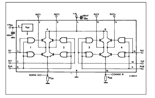
I recently took another look at the L298 since some students were having problems (due to the commonly discussed high V_CE-on of the combined high side and low side drivers). One thing that struck me as weird is that the L298 uses NPN transistors as both high side and low-side drivers.

How does the high-side driver actually switch when VB < VE < VC? For example, if Vs is 40V and Vss is only 5V, the base (as the diagram is drawn) is lower than both collector and emitter voltages, so I don't see how the high-side transistors are doing anything (other than maybe pulling the load up to ~4V and getting hot). Is there some base-drive logic that's not drawn in the diagram? I was thinking that it's possible the high side AND gates are actually open-collector, so that normally they would be pulled up to Vs through an internal resistor which is not drawn. That would sort of work - but in that case, the current gain is still limited by the inherent diode drop in the transistor, which also would change depending on the load current...

Is there a good analysis of the actual operation of the L298 h-bridge? It seems to be more complicated than it looks.

I've attached the diagram from the datasheet for convenience. enter image description here

Zuofu
  • 4,168
  • 2
  • 21
  • 36

1 Answers1

4

I think you'll probably find your answer in the L293 data sheet - it's the lower-power version of the 298 (without the heatsink). Here's what the 293 output stage looks like: -

enter image description here

The 293 (and I strongly suspect the same for the 298) has a PNP transistor that is much more conveniently driven from a low side logic signal.

I'm fairly sure the two devices work internally the same way - they have pretty-much exactly the same poor output specification. The diagram shown in the 298 spec "hints" at the limitations inherent in this type of H bridge because of the use of NPN transistors at the "top" and darlington transistors at the "bottom". See also this for alternative devices using MOSFETs.

Andy aka
  • 434,556
  • 28
  • 351
  • 777
  • The PNP devices are typically pretty horrible, being of "lateral" construction, they have very low \$h_{FE}\$ so they can't realistically be used directly. Typical drops are 1.35/2.0V (source) and 1.2/1.7V (sink) for 1A/2A. – Spehro Pefhany May 05 '14 at 18:48
  • Ah, okay, that makes a lot more sense that the "NPN transistors" in the L298 datasheet are actually not-really NPN transistors. I guess it's a Sziklai pair...or something similar. – Zuofu May 05 '14 at 18:50