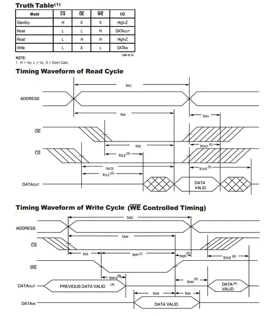
CE (chip enable) may also be named CS (chip select), as it is in the timing diagrams below. The others are WE (write enable) and OE (output enable). These are all active low (indicated by the overbar), but since that can't be done with ASCII characters I will use a # suffix in the text below, e.g. CS#.
CE#/CS# is normally high. To read the RAM, the address of the byte to be read out is presented on the address lines, A0 through A10, not shown. Eleven address lines means the chip can hold 2K bytes. CS# is then brought low, followed by OE# (output enable), which enables the output on the eight I/O lines (they are normally tri-stated when OE# is high).
After a delay known as the access time (maximum of 15 ns for this chip), the contents of the byte in memory will be available on the I/O lines. After reading the data, CS# and OE# can be brought high again.
To write a byte, the address of the byte to be written to is presented on the address lines. CS# is once again brought low. The data to be written is put onto the I/O lines, and WE# (write enable) is brought low for a minimum of 12 ns. WE# then is brought high again, and on the rising edge of WE# the data is written into memory.
If you look at the Truth Table below, you will notice that the I/O lines are tri-stated if either the CS# is high, or both OE# and WE# are high. This is to allow multiple chips to be wired with their I/O lines in parallel.
Let's say you wanted to make an 8K memory using four chips. Two additional address lines A11 and A12 would be decoded into the four CS# lines needed, for example using a 2 to 4 decoder like the 74HCT139. When one chip is selected for reading out, with CS# and OE# both low, its I/O lines are set up as outputs and drive the bus, and the other chips are tri-stated so they don't try to drive the bus themselves. Likewise for writing, when one chip has CS# and WE# low, its I/O lines are set up as input lines, and the other chips stay out of the way.