Clarification: Cadence (the company) markets two separate tools for schematics entry: HDL and OrCAD. These two tools are very different because they originate from different developments/acquisitions.
The details below refer to OrCAD
This question comes up in both the schematic entry phase, and also in the PCB layout phase. I'll explain both cases. These answers are for version 16.6 (S025), but I expect they'll work for your version.
Schematic Entry
In this case, general Grid settings can be found in the toolbar, by clicking on Options -> Preferences. In the screen that comes up, choose the "Grid Display" tab:
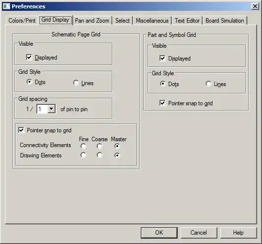
You can see the display and snap setting. If the grid is still not appearing, the click on Tools, and make sure the following settings are selected:
When moving a component or wire, the trick is to make sure you don't place pins or wire vertices onto other connection points. Once you pick up the part (by clicking and holding), you will see red warning flags as you move the part over other components. If you drop the part when these flags are displayed, it will make automatic connections for you. In the following picture, I am holding the LED over the wire. The red circle is the warning that an automatic connection will be made:
PCB Layout
The Grids setting are found in Setup -> Grids. You can set each layer to a different grid spacing, and it will automatically change depending on your active layer. Make sure you check the box in the upper-left corner:
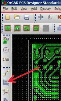
As far as moving traces (or vias), you'll want to use the Slide command:
Unfortunately, this doesn't work for components. Cadence tells me that the only way to move components without disconnecting the traces is to enable "Stretch Etch" in the Move options. First go into Move mode:
Then, click "Stretch Etch" in the options screen (which is hidden by default, on the right-hand edge of your screen):
Use Stretch Etch with care; it doesn't always do what you want, and can get messy :)
As of version 16.6, there is a "Slide Etch" option as well, although I haven't played with it yet...
I hope this helps!