4

What is the function of the two resistors arranged in parallel with the transistor? Do they also limit the current to the transistor?

enter image description here

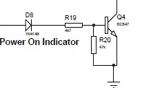
The full circuit is this:

enter image description here

PeterJ
  • 17,131
  • 37
  • 56
  • 91
user39428
  • 61
  • 4
  • 2
    At most one of the resistors is in parallel with the transistor. – Olin Lathrop Mar 29 '14 at 12:57
  • @OlinLathrop That would be a duplicate, were it not for D8. The answer is still *mostly* the same, but I think it's different enough to not be a duplicate. – Phil Frost Mar 29 '14 at 13:03
  • 2
    @Phil: The OP never asked about D8. If you understand the answer to the other question, then you should also understand the answer to this one just as well. – Olin Lathrop Mar 29 '14 at 13:06

3 Answers3

3

Given that R19 is so much smaller than R20 I'd say the main purpose of R19 is to limit the current into the base of the transistor. This of course needs to be done in all grounded-emitter configurations.

The forward volt-drop of B-E is about 0.7V and it's quite easy to destroy a BJT without this current limiter.

R20 is less obvious - some engineers will put a resistor here because they may feel it is needed but in a lot of cases it isn't. The argument for its inclusion is debatable. If the application of the circuit were better known it might be possible to explain this resistor a bit better.

Dave Tweed
  • 168,369
  • 17
  • 228
  • 393
Andy aka
  • 434,556
  • 28
  • 351
  • 777
  • @dave why it can't be common emitter ? – tollin jose Mar 29 '14 at 11:42
  • @tollin: There are plenty of common-emitter transistor configurations that have a resistor in the emitter circuit to provide negative feedback. Such circuits do not need external series resistance in the base circuit. – Dave Tweed Mar 29 '14 at 11:48
3

R20 can have two purposes. Without analysis of the full circuit and its purpose I can't say whether either is applicable here.

  • without R20 ALL current through R19 will flow through the transistors BE and will thus be amplified. Especially when the pull-up resistor has a high value (in this case it is only an interal weak pull-up??) this can cause a problem. In a circuit without the diode, R20 prevents the transistor from switching on at ~ 0.6V, which can be a valid 0 output from a previous stage.
  • R20 makes the transistor switch off faster, especially in the presence of the diode (as Phil points out, without the diode the current through R19 could discharge the base. With the diode it can't).
Wouter van Ooijen
  • 48,407
  • 1
  • 63
  • 136
  • 1
    Maybe worth pointing out that the reason the diode makes switch-off slower is that the diode blocks what would otherwise be the path for the current necessary to discharge the base capacitance. – Phil Frost Mar 29 '14 at 12:57
  • R20 also functions the same as a "pull-down" resistor in logic circuits, since this transistor circuit is designed to have only two states, off and saturated. – tcrosley Mar 29 '14 at 16:53
  • @tcrosley: that loosely some the first case reason I mention, but, contrary to a CMOS input, a transistor is off when the base is left unconnected. In the absence of any current there would not be any need for the pull-down resistor. – Wouter van Ooijen Mar 29 '14 at 17:01
  • @WoutervanOoijen -- if left unconnected, can't they pick up noise? You'd have a little antenna sitting there. I thought that was the reason it is always recommended to tie TTL inputs (which are BJT's) either high or low? – tcrosley Mar 29 '14 at 17:13
  • Real old-fashion TTL or LSTTL inputs can be left open without problem (they will behave as if tied to Vcc). The required current to pull them down is substantial (much higher than the current to switch the transistor in this question), when you get that amount of current by inductive or capacitive coupling you are in a very peculiar environment! For any CMOS logic the situation is very different: their input resistance is so high that they can easily pick up a signal when left open. – Wouter van Ooijen Mar 29 '14 at 17:29
2

R19 is picked to set the base current of the transistor when the output of the SIM340C is "high".

The design equation would be: R19 = \$V_{OUT} - V_{BE} - V_{F} \over I_B + (V_{BE}/R20)\$ Where \$V_F\$ is the forward voltage of the 1N4148 at the design output current and \$V_{BE}\$ is the base-emitter voltage of the transistor at the design base current, \$V_{OUT}\$ is the STATUS output voltage when supplying the design output current, and \$I_B\$ is the design base current.

You would normally pick the base current to ensure saturation of the transistor under worst case conditions. A "forced beta" (ratio of collector current to base current) of 20:1 might be reasonable. So if the collector current is 4mA, you might want the base current to be a couple hundred uA. In the case of the recommended circuit, it is around 200uA.

R20 is picked to pull the base low and reduce leakage through the transistor when the LED is 'off'. It's not critical, but making it around an order of magnitude bigger than R19 or more means that most of the current gets to the base when the transistor is "on" (and that current is much smaller again than the LED current, so little is wasted). It also makes the transistor switch 'off' faster, as Wouter points out, but that's not that important for a visual indicator LED.

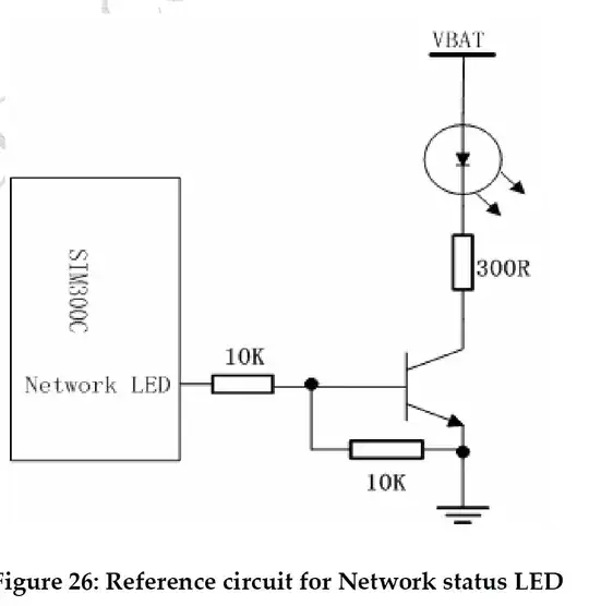
D8 appears to be there because the designer did not understand the reason for the diode in reference designs that drive a beeper. It's not required. The recommended circuit for the status indicator from the reference manual is shown below:

enter image description here

Spehro Pefhany
  • 376,485
  • 21
  • 320
  • 842