3

There are many "process technologies" that exist to fabricate circuits on silicon. They are mainly differentiated based on size of some feature. Here is the list of them:

10 µm – 1971
3 µm – 1975
1.5 µm – 1982
1 µm – 1985
800 nm – 1989
600 nm – 1994
350 nm – 1995
250 nm – 1997
180 nm – 1999
130 nm – 2002
90 nm – 2004
65 nm – 2006
45 nm – 2008
32 nm – 2010
22 nm – 2012
14 nm – 2014
10 nm – est. 2015
7 nm  – est. 2017
5 nm – est. 2019

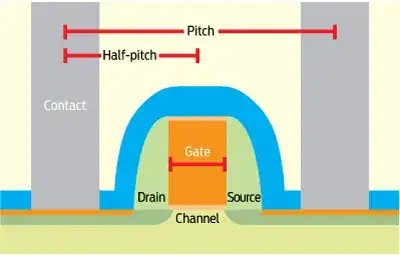
What I wish to know is, what precisely do these numbers refer to e.g the 90nm that was reached in 2004, what does it precisely mean?

I think it has to do with some dimension of the transistor that is fabricated but do not know the details. So what does it mean?

quantum231
  • 11,218
  • 24
  • 99
  • 192
  • Look I want to understand e.g for the 90nm process technology, what is 90nm when we make a die? – quantum231 Mar 17 '14 at 14:18
  • As I mentioned in my reply... 90nm would be the distance between separate CMOS on a die –  Mar 17 '14 at 14:24

3 Answers3

3

The nanometer number on memory chips generally refers to the smallest "half-pitch" between identical features on the chip, as in this illustration from an IEEE article.

enter image description here

By this definition, a fairly fine-pitch PCB with 0.004" traces and spaces would be defined as 100 micron (100,000nm).

On microprocessors, it refers to the "node number" (the smallest feature). A CPU with a 32nm node might have a 50~56nm half-pitch, and a 22nm chip might have a 34nm half-pitch.

Spehro Pefhany
  • 376,485
  • 21
  • 320
  • 842
  • That's a good article, but the OP is asking about the old-style "node" numbers, which correspond to minimum feature size, which would typically be the minimum width of a gate line (channel length) or the spacing between adjacent gates. – Dave Tweed Mar 17 '14 at 14:53
  • @DaveTweed You're right, I'll re-write it. – Spehro Pefhany Mar 17 '14 at 14:58
2

It refers to half the distance between neighbouring details on the die (ie between two CMOS)

0

Those are standard units, not specific to electronics or semiconductor manufacturing.

The "m" stands for meter, and the letter before it is one of the standard prefixes denoting a power of 1000. Here are some common prefixes:

Prefix  Name        Multiplier
------  ----------  ----------
     G  Giga        109
     M  Mega        106
     k  Kilo        103
     m  milli       10-3
     µ  micro       10-6
     n  nano        10-9
     p  pico        1012

So "22 nm", for example, means "22 nano-meters". This is the minimum feature size of that technology.

Olin Lathrop
  • 310,974
  • 36
  • 428
  • 915