I know that with usual through hole components we can attach heatsinks etc. But how does it work with surface mount components? Is having a copper plate around the component the way to go? How do we go about calculating the area required?
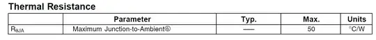
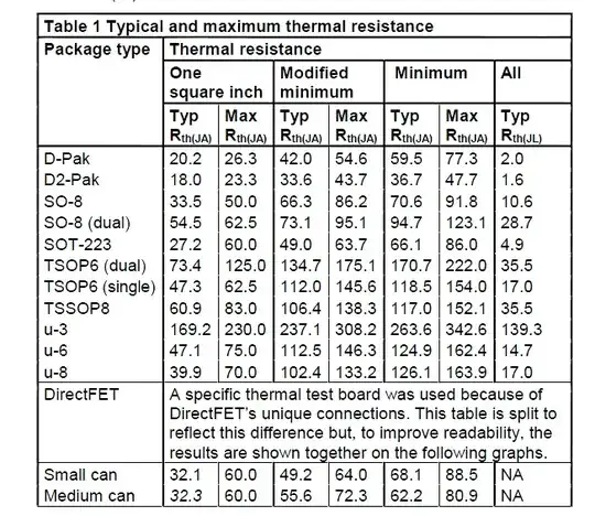
In particular I am looking at this SO8 package surface mount switching power MOSFET IRF7452(datasheet). I am sure that it requires an external form of heatsinking other than its case. But I don't seem to see it written anywhere on the datasheet? How do you know how much maximum heat energy can be dissipated using the case of the MOSFET itself? How does one go about designing the heatsinking for something like this? Would the copper plane be connected to the ground? Which part of the chip will contact and transfer most of the heat?
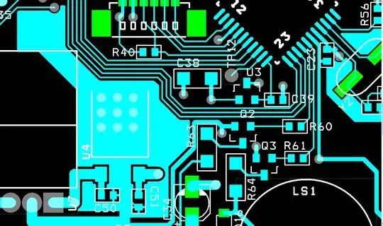
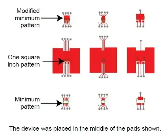
 (source
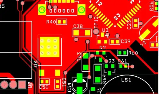
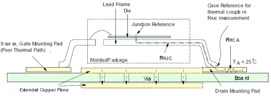