7

I have updated this question with the suggestions in comments and answers. Make sure you read everything.

I want to make a PCB for a switching regulator (buck converter). It's a TL5001-based regulator, but this doesn't really matter since the layout is about the power stage, which is common to any regulator of this type.

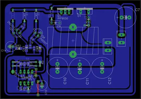
Here's what I got so far:

enter image description here

The basic idea is to make a star ground. The center of the star is the connector on the right, which is the output connector. I tried to keep traces away from the inductor (it's a toroid but I'm not sure how it affects nearby traces. C7 is the input capacitor, placed near the MOSFET, to provide enough current during switching. The small components (C8/R10 and C9/R12) are snubbers for the catch diode and MOSFET. Previous experiences with this circuit have shown I need a snubber, or else I get a ringing about 15MHz. 10nf+56R solves this. The datasheet only talks about a snubber at the diode, not the MOSFET.

There is no trace between the coil and the diode (thin yellow line) because I couldn't find a way to run a low-impedance trace there, so I'll just solder a thick piece of wire in place.

The rest of the circuit is the PWM controller (TL5001) and the MOSFET driver (2N2222/2N2907).

The feedback pin of the IC is not connected, but it's a solder pad (LSP1 on the left) because I would prefer to run a remote sense wire.

Traces will be rounded once i get a more definitive layout, to reduce EMI (I don't know if that's even necessary)

As you can see, the board is also single-layer, as I don't have the capability to do double layer boards at home, so ground plane layer is out of the question

I would prefer answers to stick to the topic here which is the LAYOUT of the board. I'm not interested in answers regarding:

  • The converter IC: Yes, I know there are better ones that are faster, cheaper, and every other adjective you can throw at it. But I have a few TL5001s.
  • The MOSFET driver: Yes, i know there are dedicated MOSFET drivers. But this pair of 2222/2907 does the job I need.
  • Double layer boards: as I said before I don't have the capability to do double-layer at home.
  • "But you can have them made for cheap!": Yes, I know. I also know I could just buy a converter, and even save myself the headaches. But I CAN'T have boards made (3 month delays at the post and import restrictions).
  • Anything unrelated to layout of the board.

EDIT:

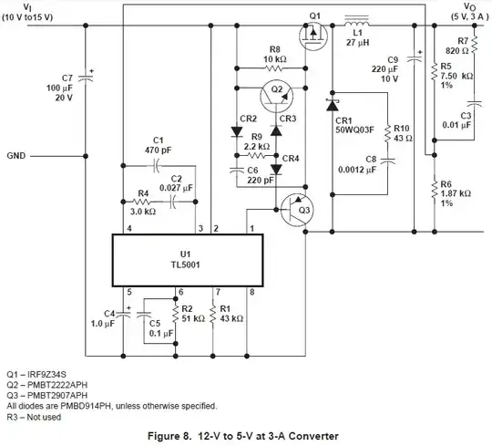
Here's a schematic. Vout for me is variable 2-12V, Iout is 0-5A.

enter image description here

EDIT 2:

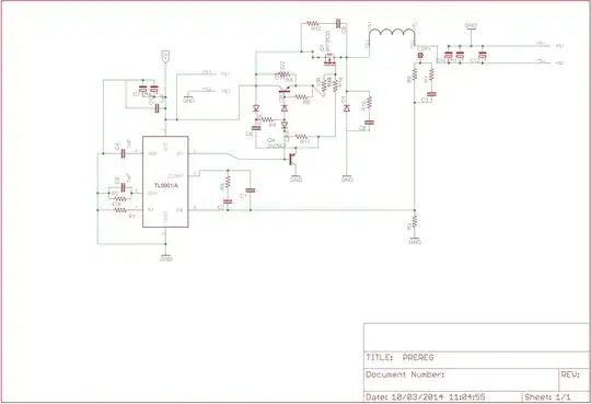
Here's the schematic corresponding to the layout. There are minimal component changes (addd R13, R14 for slew rate limit, R12, C9 for snubbing mosfet).

enter image description here

Edit 3:

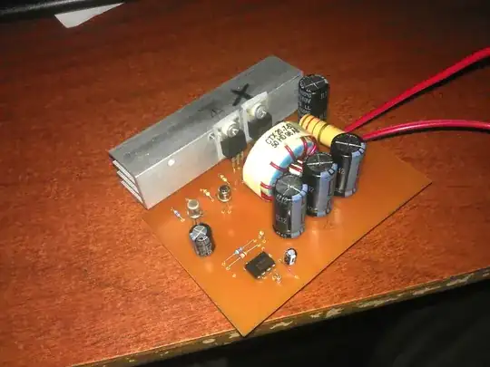
This is the final board I built:

enter image description here

Picture of the finished board:

enter image description here

And here's a video of it in action: http://youtu.be/NXNk-duzGrI

Chris Laplante
  • 2,151
  • 1
  • 24
  • 32
hjf
  • 1,069
  • 2
  • 14
  • 24
  • I'd be concerned about the heat coming off Q1 affecting the components around it. – Ignacio Vazquez-Abrams Mar 10 '14 at 05:47
  • A circuit diagram may help. Maybe C7 is a bit close to Q1, warming it up, decreasing its lifetime. – jippie Mar 10 '14 at 05:47
  • 1
    What are the trace sizes? I would think a "quasi-ground" plane on the same layer might work better because it's larger and not only would conduct better, but would allow the return currents to flow as needed and would also help with heat dissipation. – helloworld922 Mar 10 '14 at 05:54
  • @IgnacioVazquez-Abrams, jippie: Yes, I always try to keep electrolytics away from heat sources. But in this case, I've built a previous version and it really doesn't get that hot. The heatsink just "feels warm". – hjf Mar 10 '14 at 05:58
  • @helloworld922 you mean just a ground pour on that side? I'm worried about ground loops happening. Trace size is 2.54mm and I'll reinforce with wire soldered on the trace if needed. – hjf Mar 10 '14 at 05:59
  • @hjf Hello :) What are ground loops and how will they happen? – abdullah kahraman Mar 10 '14 at 07:10
  • Do you not have UPS/DHL service at your home? You will be *much* better off ordering at a place like iteadstudio/seeedstudio and getting a properly made 2 layer board for this kind of stuff. Having a ground plane alone will make this design 10x better. Also, having a star ground really doesn't serve any purpose in a dc/dc converter, esp. a super old low frequency inefficient beast like this. Just pour the ground as much as possible. You want minimum ground impedance! – user36129 Mar 10 '14 at 08:09
  • @user36129 UPS/DHL/FedEx and other can be prohibitively expensive even when available. Not everyone has the luxury cheap courier services. – AndrejaKo Mar 10 '14 at 08:48
  • @AndrejaKo: that is why I am asking. Almost all countries and regions are serviceable by them nowadays, it is very rare to find people that cannot cheaply get professionally made PCBs. And it improves both enjoyment and productivity so much that this is definitely the first step to try to undertake on this design. If not, we can always fall back to homemade stuff and improve layout there. But not before we explore the professional route. – user36129 Mar 10 '14 at 09:25
  • @user36129 I completely disagree! The professional route has been ruled out in the question and sufficiently explained. Furthermore it can definitely rule out any "enjoyment"! For example, shipping from China to me via UPS would be around $80. This alone can bring the order into range where it has to formally go through customs, so a forwarding agent has to be used giving additional $70-$80 for agent's fees plus customs and VAT. All this for a board that costs $5 to make. Of course, this is all assuming that online payment is possible in the first place. – AndrejaKo Mar 10 '14 at 09:32
  • 4
    @user36129 Shipping from UPS/DHL/Fedex and any others is, minimum, $100. International packages to Argentina are now limited to 2 a year. There is a 50% import tax, and a 35% tax on "international payments". So while I COULD order from abroad, it's obvious why I won't. (There are PCB manufacturers in Argentina but the minimum order is 500) – hjf Mar 10 '14 at 13:35
  • 1
    I think you need to sort out the circuit references on the artwork. I can't see R5 or R7 anywhere and on the circuit why don't these connect to the output of the coil? This is basic stuff dude. You should be getting this right and not generating ambiguities. OK if you a beginner you are forgiven. – Andy aka Mar 10 '14 at 15:38
  • With regards to EMI, I would definitely not worry about rounding the traces. – dext0rb Mar 10 '14 at 15:46
  • @user36129 I am sorry but I will have to agree with AndrejaKo on this. $50 is not cheap. – abdullah kahraman Mar 12 '14 at 07:38

2 Answers2

7

No, it's not a good layout. Star pointing ground returns is a good idea but I'd use a double sided PCB for best layout. The circuit doesn't help you get the best layout either. Pin 8 of U1 should ideally directly connect to the grounds on the big smoothing capacitors and take no current up any of its length that would flow into those three big caps. U1 has to "measure" the output voltage via a potential divider and it needs a stable 0V reference to do this.

Incidentally, the circuit diagram does not match the layout - where are the feedback components R5 and R6? Where is CR1? I've already worked out that C9 = C10/11/12 but you are doing things that I can't see on the circuit. This is bad dude. OK I can see that CR1 has become D1 but this needs to be right up at Q1 to work effectively unless you don't mind replacing Q1 now and then and interfering with your neighbors AM radio.

In short, you may get away with 1 sided PCB but more work needs to be done.

Please post a circuit that matches the artwork as well - we are not paid to help so don't make life difficult for us.

Andy aka
  • 434,556
  • 28
  • 351
  • 777
1

Many switched regulators include example layouts, such as the suggested alternative part TPS40200. http://www.ti.com/lit/ds/symlink/tps40200.pdf . The datasheet shows the evaluation module layout and a suggested layout. If you copy that layout then your circuit will probably work.

One thing I found interesting is that switched regulator layouts tend to use copper fills instead of traces to connect high-current paths and simultaneously provide some heat sinking. For example in your layout C10-C12 and the large rectangular component could sit on top of a solid rectangle of copper. Keep in mind that the electrons will take the lowest impedance path.

joeforker
  • 5,596
  • 10
  • 38
  • 59
  • Great! these layouts are mostly for SMD but I think i can get some "inspiration" from these as well. – hjf Mar 10 '14 at 15:27