7

I have developed an application by using STM32F4-Discovery development kit. Now code is mature and I need to build a custom circuit.

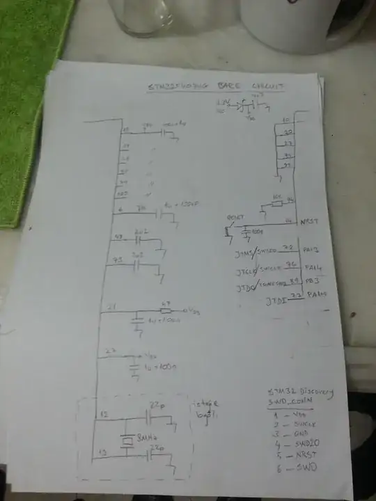
I started building the bare circuit first:

STM32F407 bare circuit test pcb

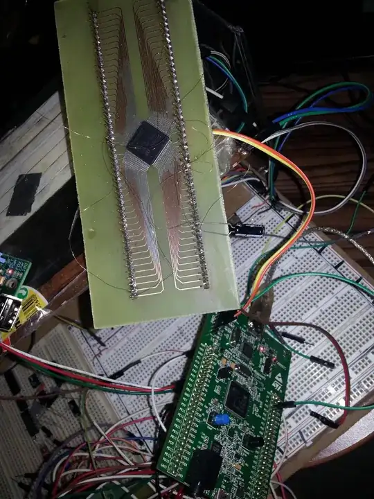
I soldered the chip on the pcb via a standard 30 Watts soldering iron with a technique like in this video: http://www.youtube.com/watch?v=6YU3v_w7x7o

Since I didn't get the point of connecting 1uF//100nF capacitors between every VDD-VSS pin, I only connected a 4.7uF capacitor to the entry point of power lines.

My pin connection is as follows:

  • VDD <- 11,19,28,50,75,100,21,22,6
  • GND <- 20,10,27,74,99
  • 2.2 uF cap is between 49 and GND
  • 2.2 uF cap is between 73 and GND
  • 10 K resistor is between 94 and GND
  • MCU.72 is connected to STM32F4-Discovery.SWD_connector.4
  • MCU.76 is connected to STM32F4-Discovery.SWD_connector.2
  • MCU.VDD is connected to STM32F4-Discovery.3V
  • MCU.GND is connected to STM32F4-Discovery.GND

Question:

I'm expecting to connect the MCU via STM32F4-Discovery's ST-Link/V2, but ST-Link utility is not being connected. I'm not able to get a heartbeat with the MCU.

What is the point I am possibly missing?

Edit:

(moved to the answer)

ceremcem
  • 1,386
  • 17
  • 35
  • What is your question? I read "I did this and used that" but I have no idea what you expect and what didn't happen. – Andy aka Mar 06 '14 at 23:56
  • "I'm expecting to connect the mcu via STM32F4-Discovery's ST-Link/V2, but ST-Link utility is not being connected. " – ceremcem Mar 06 '14 at 23:59
  • Nice cut and paste dude – Andy aka Mar 07 '14 at 00:01
  • Maybe the question part was not clear. I edited also. – ceremcem Mar 07 '14 at 00:06
  • 6
    Bypass caps are more critical than you are imagining. You should follow the data sheet closely on their size, count, and placement. Similarly, routing of power and ground is going to be as critical. Those long traces have a lot more inductance than you'd expect. You also need to make sure you've configured the debugger for SWD and not JTAG, and that you've wired any floating pins on the debugger's connector appropriately. – RBerteig Mar 07 '14 at 00:18
  • Ok, then I'm making another test pcb and place all of the 1uF//100nF capacitors. See you in the morning. – ceremcem Mar 07 '14 at 00:32
  • @RBerteig , please see the edit. – ceremcem Mar 07 '14 at 19:03
  • 2
    What is supply voltage? How much current is being drawn? What is the voltage of the reset pin? What is your clock setup? (The discovery board appears to have a crystal connected, do you need different settings to use the internal RC oscillator?) – markrages Mar 07 '14 at 19:10
  • I_mcu=2.8mA, VDD=2.75V, V_NRST=2.75V . I think these values are normal. The mcu datasheet says that if external oscillator fails, it switches back to the internal oscillator and if configured so, an interrupt is generated. So, without an external oscillator, this circuit should work. I'm only trying to get a connection via ST-Link utility, nothing more. – ceremcem Mar 07 '14 at 20:42
  • Wait! I rechecked the mcu pins' solder, and guess what! SWCLK pin was not connected. I resolder the pin and everything works as expected. Thank you! – ceremcem Mar 07 '14 at 21:00

1 Answers1

16

Regarding @RBerteig's advice, I made following circuit:

Test circuit 2

Differences:

  • There are 1uF+100nF capacitors connected all the VDD and GND pins (as close as possible)
  • Short routes

Temporary Problem: This circuit was not working. I was not able to connect it via ST-Link utility.

Solution: I checked the pins and one pin (SWCLK) was not connected to the PCB. When I soldered the pin, everything works as expected.

Edit

Here is the bare circuit schematics:

(note: isteğe bağlı means optional)

bare circuit

ceremcem
  • 1,386
  • 17
  • 35
  • Would you mind sharing the schematic with us? – Chimera Jan 09 '15 at 20:12
  • Sure: https://ceremcem.net/cloud/f/bae82d2a09/ – ceremcem Jan 10 '15 at 00:07
  • Are those 5 square through hole pads on the right hand side of the board for SWD? Thanks for the schematic link, it appears to be invalid though. – Chimera Jan 12 '15 at 16:58
  • Sorry for the link, I updated the answer accordingly. Yes, the pads are for `Vdd`, `Gnd`, `SWCLK`, `SWDIO` (and one more thing that I can not call right now) – ceremcem Jan 13 '15 at 11:47
  • 8
    +1 for solving it yourself, then taking the time to follow up and show us the solution. Second PCB is much nicer. – pjc50 Jan 13 '15 at 11:58