Okay, so I was a bit of an idiot while designing my PCB. The specifications of my PCB fab were 6/6 mil trace/space, and the boards did not meet this. So, below is the design for the PCB:
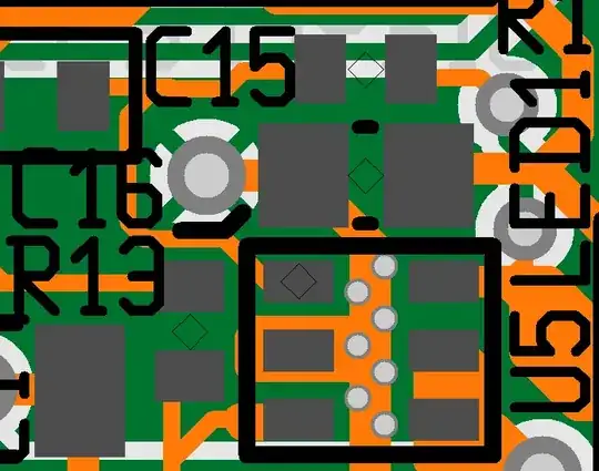
The trace going to C16 (a ground) is way too close to the pad which is connected through a trace to an inductor (it's a switch mode buck converter.) This basically connects the +3.3V line next to the filter capacitor to GND, shorting it. I verified this with the continuity test on my multimeter.
My PCB:
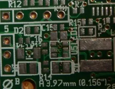
I have already bought 10 PCBs, so I'd like to know if it's possible to hack these and repair them. I'm okay with having to provide them with an external 3.3V source; in future, I'd like to get the converter working, but it's the rest of the circuit which is important.
Obviously I won't make this mistake in the next version... I might actually run the DRC. This is only for development.